|
|||||||||||||||||||||||||||||||||||||||
|
|
|||||||||||||||||||||||||||||||||||||||
       |
Letters Vol. 7, No. 12, pp. 37–43, Dec. 2009. https://doi.org/10.53829/ntr200912le1 High-speed, High-reliability 0.5-μm-emitter InP-based Heterojunction Bipolar TransistorsAbstractWe have developed 0.5-μm-emitter InP heterojunction bipolar transistors (HBTs) towards over-100-Gbit/s integrated circuit applications. The HBTs incorporate a passivation ledge structure and tungsten-based emitter metal to achieve high reliability at a high collector current density. The fabricated HBT exhibits a current gain of 58, ft of 321 GHz, and fmax of 301 GHz at a collector current density of 4 mA/μm2. The results of accelerated life tests predict an activation energy of around 1.5 eV and the extrapolated mean time to failure is over 108 hours at a junction temperature of 125ºC. 
1. IntroductionThe remarkable high-speed performance and high breakdown voltages of InP-based heterojunction bipolar transistors (HBTs) make them promising candidates for use in ultrahigh-speed integrated circuits (ICs) for future optical fiber communications systems [1]. Several ICs operating at over 100 Gbit/s have already been demonstrated using InP HBTs [2]. However, for such InP HBTs to be used in practical applications, they must have excellent reliability. Some reliability data for InP HBTs has been reported in recent years [3]. In InP HBTs, degradation, such as current gain degradation, is primarily caused by surface recombination at the emitter-base periphery. An effective way to suppress the recombination current is to use a ledge structure on an external base layer [4]. Indeed, we have achieved excellent reliability in InP HBTs with a passivation ledge structure for 40-Gbit/s IC applications [5]. Our baseline HBT consists of a 300-nm-thick InGaAs collector, 50-nm-thick base, and 70-nm-thick InP emitter. The ledge structure was fabricated using the emitter layer on the external base. For the ledge layer, undoped InP is suitable because it can be easily depleted. It is also effective in reducing the emitter-base capacitance, which is advantageous for low-power operation [6]. An HBT with a 1 μm × 4 μm emitter exhibits current-gain cut-off frequency ft of 169 GHz, maximum oscillation frequency fmax of 255 GHz, and current gain of 57 at a collector current density Jc of 1 mA/μm2. The extrapolated mean time to failure (MTTF) is estimated to be over 1 × 10⁸ hours at a junction temperature Tj of 125ºC, and the degradation does not depend on Jc up to 2 mA/μm2. To build over-100-Gbit/s ICs, we need ft and fmax to be over 300 GHz. High Jc (> 2 mA/μm2) is essential to achieve these values. However, at such high-Jc operation, a sudden degradation in current gain frequently occurs [5] because of diffusion of the emitter metal, which consists of Ti/Pt/Au. Under thermal stress, Ti diffuses into the emitter, which reduces the barrier effect of Ti. Then, Au diffuses into the emitter and base, which results in sudden breakdown in the emitter-base junction. This article describes highly reliable submicrometer InP HBTs toward over-100-Gbit/s IC applications. To achieve excellent reliability at high Jc, we used tungsten-based emitter metal as well as passivation ledge structures. Here, the tungsten-based emitter metal acts as a barrier to Ti and Au. The HBT structures were laterally and vertically scaled down to provide higher ft. Section 2 explains the HBT structures and fabrication. Section 3 discusses the effectiveness of the passivation ledge structure and the high-frequency performance and presents the results of accelerated life tests, which indicate that the HBTs have excellent reliability even at Jc = 7 mA/μm2. 2. HBT structures and fabricationA cross-sectional view of the fabricated InP HBT is shown in Fig. 1. A single HBT structure was grown on a 3-inch InP substrate by molecular beam epitaxy. The epitaxial layers were vertically scaled down to halve the carrier transit time. The base and collector layers were 35-nm-thick lattice-matched p-InGaAs and 150-nm-thick InGaAs, respectively. The base layer was doped with carbon to a concentration of 5 × 1019 cm–3. The base sheet resistance was estimated to be 646 Ω/sq. by transmission line mode measurements. The emitter was 50-nm-thick n-InP. The emitter doping level was optimized to provide high Jc and high current gain [7]. In addition to the vertical scaling, the emitter width was scaled down to 0.5 μm to reduce the base-collector capacitance and collector current. The device fabrication sequence was the same as that for our baseline HBTs [5], except for the deposition of tungsten-based emitter metal to prevent Ti/Au diffusion. First, tungsten-based emitter metals were deposited, followed by photoresist mask. Next, dry etching was performed to remove the emitter metal and about half of the emitter layer. The remaining emitter layer was used as a ledge layer. The ledge thickness was about 30 nm. The surface of the ledge layer was covered with SiN film for passivation. Then, base metal was formed in a non-self-aligned manner. For the device layout, a base-pad isolation structure was used to eliminate the extrinsic base-collector capacitance at the base-pad area [8]. Finally, the devices were isolated by wet etching and passivated with benzocyclobutene.
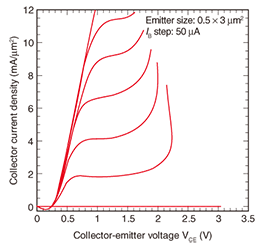
3. Device characterization3.1 DC characteristicsTypical I-V characteristics for the fabricated HBT are shown in Fig. 2. The emitter was 0.5 μm wide and 3 μm long. The HBT exhibited excellent turn-on characteristics and high current density of over 10 mA/μm2. The breakdown voltage was over 3 V.
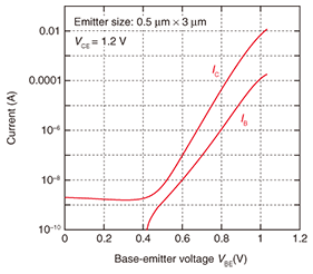
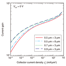
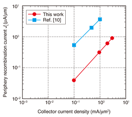
A Gummel plot for the HBT at a collector-emitter voltage VCE of 1.2 V is shown in Fig. 3. Even at a low Jc, there is no crossover in the Gummel plot. The dc current gain β was 58 at Jc = 4 mA/μm2, which is a reasonably high value. The ideality factors of the collector and base currents were 1.3 and 1.6, respectively. To investigate the effectiveness of the passivation ledge layers, we measured Gummel plots of HBTs with different emitter areas. The Jc dependence of β for HBTs with different emitter sizes is shown in Fig. 4. We used a collector-base voltage VCB of 0 V to eliminate any influence of impact ionization current at the base-collector junction. At Jc > 0.1 mA/μm2, current gain degradation due to emitter size reduction was very small. To obtain more information about the current-gain characteristics, we analyzed the base recombination current using the well-known formula [9]  where Jbi is the recombination current density under the emitter-base internal junction, JL is the emitter periphery recombination current per unit length, LE is the emitter periphery length, and SE is the junction area. JL is plotted as a function of Jc in Fig. 5. The JL values were obtained from the slope of the dependence of β–1 on the periphery-to-area ratio LE/SE using Eq. (1). For comparison, results for InP HBTs without a passivation ledge structure [10] are also shown. For the HBTs in this work, the JL value was only 0.3 μA/μm at Jc = 1 mA/μm2, which is one order of magnitude lower than that of the HBTs without a ledge structure. This indicates that the ledge layer is depleted, which suppresses surface recombination at the emitter-base periphery.
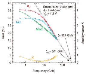
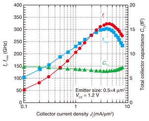
3.2 High-frequency characteristicsThe high-frequency performance of the fabricated HBTs was characterized by S-parameter measurements from 0.5 to 50 GHz using an HP8510C network analyzer. The S-parameters were de-embedded by subtracting the pad’s parasitic capacitance extracted from the measurement of an open pad structure. The current gain (h21), Mason’s unilateral gain (UG), maximum stable gain, and the stability factor are shown in Fig. 6 as functions of frequency at Jc = 4 mA/mm2 and VCE = 1.2 V. The emitter was 0.5 μm wide and 4 μm long. The ft and fmax were obtained by extrapolating h21 and UG for a line with a slope of –20 dB/decade. The ft, fmax, and total collector capacitance CTc are shown in Fig. 7 as functions of Jc. The HBT exhibited a peak ft of 321 GHz and peak fmax of 301 GHz at Jc = 4 mA/μm2. Note that CTc was 6.4 fF. The CTc value is almost the same as that of our baseline HBTs with a collector thickness of 300 nm [5], [6], which means that the emitter size reduction effectively eliminated the CTc.
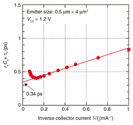
Next, we extracted the carrier transit time ΤF from the measured S-parameters of the HBT with a 0.5 μm × 4 μm emitter. On the basis of the HBT small-signal T-model equivalent circuit [11], the sum of ΤF, emitter charging time reCe, and RcCTc product is expressed as 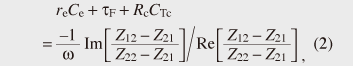 where re is the emitter dynamic resistance, Ce is the emitter-base capacitance, and Rc is the collector resistance. The Z-parameters (Z11, Z12, Z21, Z22) were obtained from the measured S-parameters. Rc was estimated from the subcollector sheet resistance and contact resistivity, which were determined by transmission line mode measurements. The sum of reCe and ΤF as a function of inverse collector current is shown in Fig. 8. By extrapolating the fitting line to 1/Ic = 0, we estimated ΤF to be 0.34 ps, which is half that of our baseline HBTs [5], [10]. This ΤF value corresponds to an average carrier velocity in the base and collector of 3.2 × 107 cm/s. An effective way to boost the average carrier transit velocity is to use a compositionally graded pseudomorphic base. We previously reported an average carrier velocity of 4 × 107 cm/s [12]. Furthermore, the pseudomorphic base is also effective in lowering the base sheet resistance, which is beneficial for obtaining higher fmax. To achieve higher ft and fmax, we will fabricate HBTs with a pseudomorphic base in the near future.
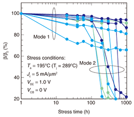
3.3 ReliabilityTo investigate the reliability of the newly developed InP HBTs with over-300-GHz ft, we performed accelerated life tests. For each test, more than ten packaged transistors were used. Each transistor was continuously biased in a high-temperature oven filled with nitrogen. The bias conditions were VCB = 0 V and VBE = 0.9–1.0 V, depending on the operating Jc. The ambient temperatures Ta were 165, 175, and 195ºC. Initial device characterization and stressed device characterization were performed at room temperature at VCE = 1.2 V using a semiconductor parameter analyzer. Here, the stressed device was cooled to room temperature before the characterization. Junction temperatures Tj of the devices were estimated from the thermal resistance, which was obtained by the method in ref. [13]. In the life tests, we used the newly developed HBT. Its emitter contact metal is tungsten-based metal and its epitaxial layer structure is the same as that for the HBT presented in the previous sections. The emitter was 0.5 μm wide and 3.0 μm long. For comparison, we also tested our baseline HBT with Ti/Pt/Au emitter contact metal for 40-Gbit/s ICs [5], for which the emitter was 1 μm wide and 4 μm long. In this section, we first explain the degradation modes of our baseline HBT and then discuss the degradation mechanism of the newly developed HBT. Changes in normalized dc current gain β/β0 of our baseline HBTs at Jc = 5 mA/μm2 are shown in Fig. 9 as a function of stress time, where β0 is the current gain before the reliability test. The stress conditions were VBE = 1.0 V and VCB = 0 V, for which Jc was 5 mA/μm2. Ta was 195ºC and Tj was estimated to be 289ºC. As we reported previously [5], the degradation of dc current gain has two modes: gradual degradation (mode 1), which is attributed to thermal degradation of the quality at the external base surface between the ledge and the base metal, and sudden degradation caused by Ti/Au diffusion into semiconductors (mode 2).
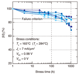
Gummel plots of the newly developed HBT after the various stress times are shown in Fig. 10. The emitter was 0.5 μm wide and 3 μm long. After the HBT was stressed for a particular period of time, it was cooled to room temperature and then the Gummel plots were measured at VCE = 1.2 V. To enable us to compare the life test results for the newly developed HBTs with those for the baseline HBTs, the Tj values of both devices should be almost the same because the degradation of dc current gain depends not on Ta but on Tj. The stress conditions were VBE = 0.98 V and VCB = 0 V, for which Jc was 7 mA/μm2. Ta was 165ºC, and Tj was estimated to be 284ºC. Although the base current gradually increased at low VBE, there was no sudden degradation in the base and collector currents with stress time.
The changes in β/β0 at Jc = 7 mA/μm2 with stress time are shown in Fig. 11. The β/β0 was obtained from the Gummel plots in Fig. 10. Although β/β0 gradually decreased, no sudden drop in β/β0, resulting from mode 2, was observed. This means that the tungsten-based emitter metal firmly suppressed the Ti/Au diffusion. Thus, the degradation of dc current gain in the newly developed HBT was mainly due to mode 1.
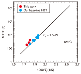
Finally, we estimated the activation energy of degradation in the newly developed HBTs. The MTTF in each life test was determined by the median rank method using a Weibull distribution. The failure criterion was a 15% reduction in β/β0. Arrhenius plots of β for the baseline HBTs [5] are shown in Fig. 12. The MTTFs of the newly developed HBTs are also plotted. The activation energy Ea for the baseline HBTs was estimated to be 1.5 eV. The newly developed HBTs had a similar MTTF tendency to the baseline HBTs. Thus, their Ea is expected to be around 1.5 eV, and the extrapolated MTTF at Tj = 125ºC is expected to be over 108 hours [14]. On the basis of these results, this submicrometer InP-based HBT technology is promising for making high-reliability ultrahigh-speed ICs.
References
|
||||||||||||||||||||||||||||||||||||||