|
|||||||||||||||||||||
|
|
|||||||||||||||||||||
       |
Special Feature: KTN Crystal Technologies Vol. 7, No. 12, pp. 32–36, Dec. 2009. https://doi.org/10.53829/ntr200912sf6 Fast Varifocal Lenses Based on KTa1-xNbxO3 (KTN) Single CrystalsAbstractNTT Photonics Laboratories has recently developed varifocal lenses that respond as fast as 1 μs, which is 1000 times faster than the conventional commercial devices. The lens structure is quite simple: a potassium tantalate niobate single-crystal (KTN) block with four electrodes on it. We were able to obtain both fast responses and large focal shifts by using this simple structure and the large electro-optic effect of KTN. These lenses are expected to be applied to new technical fields such as laser manufacturing. 
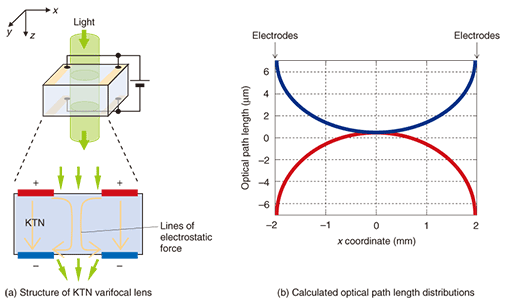
1. IntroductionA convex lens converges parallel light beams such as sunlight or laser beams into a small spot region called the focus. Although the focal position is fixed for an ordinary lens, it can be controlled in the case of a varifocal lens. An example of a varifocal lens is the lens system of a camera. It consists of several lenses, which can be moved to change the focal length of the lens system. The focus can be controlled electronically by attaching motors to the system. However, because the lenses are massive, it is difficult to move it quickly. Varifocal lenses using liquid crystals are much faster than mechanical lenses [1]. Another type of fast device is controlled by reshaping a liquid-filled flexible lens [2]. There is also a device using a phenomenon called electrowetting [3]. However, there are no commercial varifocal lenses that respond much faster than 1 ms. For applications such as laser manufacturing, the response needs to be more than one order of magnitude faster. NTT Photonics Laboratories has recently developed much faster varifocal lenses by using single crystals of potassium tantalate niobate (KTa1-xNbxO3, KTN). KTN is a perovskite-type oxide material that has a very strong electro-optic (EO) effect. The EO effect is a phenomenon whereby the refractive index of a substance is modulated by an externally applied electric field. The common conventional material is lithium niobate (LiNbO3, LN). For LN, the effect is linear, which means that the index modulation is proportional to the electric field. KTN has a very strong quadratic effect where the index modulation is proportional to the square of the electric field. With an appropriate bias electric field, the effect is a few orders of magnitude stronger than that for LN. However, crystal growth of KTN has been more difficult than that of LN. Our group has successfully developed a technology for growing large KTN single crystals with excellent optical homogeneities. In addition, we have found a phenomenon called the space-charge-controlled EO effect for KTN and have been developing an optical beam scanner utilizing it [4]. The large and fast EO effect of KTN can be also applied to varifocal lenses. In this article, we introduce our KTN varifocal lenses. With a simple device structure, we were able to obtain fairly large changes in focal length, from infinity to 1.6 m, in addition to quick responses as fast as 1 μs, which is three orders of magnitude faster than the conventional commercial varifocal lenses. 2. Principle of KTN varifocal lensesThe structure of a KTN varifocal lens is schematically shown in Fig. 1(a). It consists simply of a KTN single-crystal block together with four metal electrode stripes. A light beam is incident on the top face of the block between a pair of parallel electrodes. The beam leaves the crystal from the bottom face where another electrode pair is formed symmetrically. When a voltage is applied between the top and bottom electrode pairs, an electric field is generated in the crystal. This field is mainly formed in the two regions between the top and bottom electrodes. However, it also spreads into the gap region between the left and right electrodes through which the light travels. The field is stronger closer to the electrodes, so according to the EO effect, refractive index changes are larger near the electrodes than near the central optical axis. This index modulation, which was calculated from an electric field distribution obtained by the finite element method, is shown in Fig. 1(b). The horizontal axis is the x coordinate shown in Fig. 1(a) with the origin at the optical axis. The vertical axis shows the optical path length obtained by integrating the refractive index along the z axis. The KTN varifocal lens exhibits different behaviors for different light polarizations because of the crystallographic symmetry. For a light beam with its vibrating electric field parallel to the x axis, the optical path length curve has a peak at the center, as shown by the red line. This means that the KTN device works as a convex converging lens. For a light beam with its vibrating electric field parallel to the y axis, the curve has a trough at the center, as shown by the blue line, which means that the device works as a concave diverging lens. Hereafter, we treat only light with its electric field parallel to the x axis and thus converging lenses. For this polarization, the refractive index and the optical path length become lower near the electrodes than near the center region. Because light tends to be attracted to regions with high refractive indices, light rays are bent toward the center, and the KTN works as a converging lens.
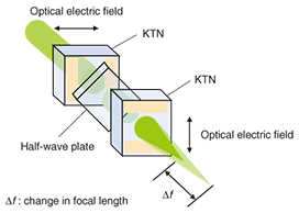
Actually, this device works not as an ordinary spherical lens but as a cylindrical lens. A cylindrical lens focuses light onto a straight line because it converges light in only one direction, while an ordinary lens focuses light onto a spot because it converges light both vertically and horizontally. The KTN varifocal lens corresponds to a cylindrical lens because it converges light only in the x direction in Fig. 1(a). However, we can construct a lens that focuses in two dimensions, corresponding to an ordinary spherical lens, by assembling two KTN lenses as shown in Fig. 2. The half-wave plate between the lenses rotates the polarization of the light so that the second KTN lens converges the light as well as the first lens rather than diverging it.
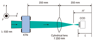
3. Focus shift performancesWe prepared several samples of a KTN single crystal block with a size of 6.6 mm × 7.0 mm × 4.0 mm. Its six faces were parallel to the crystallographic (100) faces of the cubic phase. We deposited a pair of stripe electrodes on the top 6.6 mm × 7.0 mm face by evaporating platinum. They were parallel to each other and 4 mm apart. Another pair was formed on the bottom face as shown in Fig. 1(a). The experimental setup for measuring focus shifts by the KTN lens is shown in Fig. 3. The light source was a 532-nm-wavelength laser whose beam diameter was 3 mm. We observed intensity distributions of the converged light by using a CCD (charge coupled device) image detector at various positions on the optical axis. To enhance the confinement of the laser power at the focus, we used a glass cylindrical lens whose focal length was fixed to 250 mm. A KTN varifocal lens itself can change the focal length from infinity to about 1 m, but the minimum beam width is as large as 0.35 mm. Although the fixed cylindrical lens reduced the focus shift range, it improved the minimum beam width by reducing it to about 0.1 mm. Light intensity distributions at L = 0 and 40 mm were measured. L = 0 mm is the focal position of the fixed cylindrical lens and L = 40 mm is 40 mm nearer the cylindrical lens.
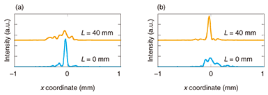
The measured light distributions are shown in Fig. 4, where the horizontal axis is the x coordinate in Fig. 3. Fig. 4(a) shows distributions without any voltage applied to the KTN lens. In this case, because the KTN lens did not do anything to the laser beam, the light was focused by the fixed cylindrical lens to the focal position at L = 0 mm. Thus, the blue line shows strong power confinement at the center, whereas the orange line shows that the light was defocused at L = 40 mm. Fig. 4(b) is for an applied voltage of 1000 V. The sharp peak in the orange line indicates that the focus moved toward the KTN lens by 40 mm, while the light at L = 0 mm was defocused.
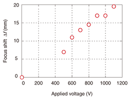
The voltage dependence of the focus shift is shown in Fig. 5. It indicates that, when voltage was applied, the KTN single crystal worked as a convex converging lens and the focus was moved towards the KTN. As the sample used for Fig. 5 was different from the one used for Fig. 4, the focus shift performance was also different. The shift Δf should theoretically be proportional to the square of the applied voltage. The measured voltage dependence deviated slightly from the theory at voltages higher than 800 V. We are now studying this deviation and will be reporting the result in the near future.
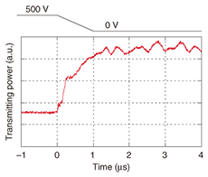
We also evaluated the time responses. We obtained the data for Figs. 4 and 5 by using a CCD, as shown in Fig. 3. However, because its frame rate was about 20 frames per second, we were not able to evaluate responses faster than 5 ms. We placed a pinhole at the focus for 0 V and observed light passing through it by using a photodiode (PD) in order to obtain fast time responses. We chose a 50-μm pinhole, which is smaller than the minimum width (0.1 mm) of the confined light. When the focus was close to the pinhole, the light intensity there was high and the PD output was high. When the focus was far from the pinhole, the light was defocused at the pinhole and the PD output was low. A time response of the PD output is shown in Fig. 6. At t = 0, we switched off the voltage, causing it to fall from 500 V to 0 V. The output rose as the status changed from defocused to focused. This shows that the response time was less than 1 μs. The response includes a small vibrating component with a period of about 0.5 μs. This was caused by electrostriction, which is a phenomenon whereby strains are induced by electric fields and the strain is proportional to the square of the electric field [5]. The vibration in the output was due to mechanical vibrations caused by quick strain changes in the KTN crystal with the abrupt switching off of the voltage. When we changed the applied voltage faster than 1 μs, the vibration as a noise source became larger. We can expect even faster responses once the mechanical vibration has been successfully eliminated.
4. ConclusionWe have developed varifocal lenses based on KTN single crystals having a simple structure. Focus shifts as large as 40 mm were observed with a cylindrical lens with f = 250 mm, which means that the KTN device itself changed the focal length from infinity to 1.6 m. As the lens utilizes the EO effect, the feature of this device is its high speed. It responds as fast as 1 μs, which is about three orders of magnitude faster than the conventional commercial varifocal lenses. This high speed will lead to KTN varifocal lenses being applied to new technical fields such as laser manufacturing. References
|
||||||||||||||||||||