|
|||||||||||||||||||||||
|
|
|||||||||||||||||||||||
       |
Special Feature: Silicon Photonic Technologies Leading the Way to a New Generation of Telecommunications Vol. 8, No. 2, pp. 6–10, Feb. 2010. https://doi.org/10.53829/ntr201002sf1 R&D Trends in Silicon PhotonicsAbstractSilicon photonics could, by integrating optical and electronic circuits on silicon, reduce the costs and power consumption of networks while meeting the need for advanced functionality. Further expansion of the information society will require optical networks with greater capacities and higher speeds and high-performance electronic circuits with faster operation. However, these developments will increase costs and power consumption. This article overviews research and development trends and introduces the other articles in this Special Feature. 
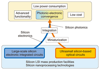
1. IntroductionToday’s advanced information society has reached its present state through the combination of large-capacity, high-speed communications networks for transmitting information and electronic circuits for processing that information rapidly. This mechanism is supported by optical communications technology, which provides large-capacity and high-speed communications, and by silicon integrated electronic circuit technology, which provides high-speed, large-scale integrated circuits (LSIs). In particular, the remarkable developments in mass-production technology that exploits the superior material properties and fine-processing characteristics of silicon have made possible the low-cost production of LSIs (on the order of ten million units) and driven the widespread use of high-performance appliances. If the advanced information society is to continue to expand, optical networks must offer even greater capacities and higher data-transfer speeds and the processing capacity of electronic circuits be improved. However, from an economics viewpoint, greater functionality must be accompanied by lower costs. Furthermore, from the viewpoint of reducing the load on the global environment, which is an issue of growing concern, a variety of problems must be solved. These include the increase in the power consumed by LSIs themselves due to faster electronic circuits, the power consequently consumed by the huge amount of equipment using LSIs, and the dramatic increase in the power consumed by the networks interconnecting that equipment. As shown in Fig. 1, silicon photonics is a technology that aims to achieve convergence between photonics and electronics (photonic-electronic convergence). The plan is to use silicon, which has been the base material for electronic circuits, to replace the various non-silicon materials currently used to form optical devices and to integrate ultrasmall silicon optical circuits and silicon electronic circuits on the same chip. The use of silicon lets us utilize the advanced mass-production facilities that have enabled the low-cost production of electronic circuits. Therefore, it is expected to provide an economical benefit by achieving advanced functionality in optical devices that support the network at a lower cost. It is also expected to suppress the total power consumption in network systems through the development of photonic-electronic convergence equipment that consumes less power while achieving even more advanced functionality.
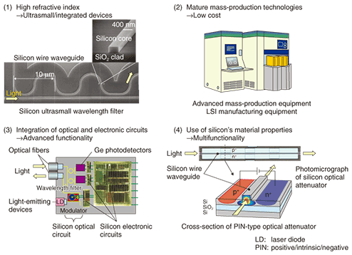
This article begins by describing the technical features and applications of silicon photonics. It then reports on worldwide research and development (R&D) trends in silicon photonics and finally describes NTT R&D activities toward the application of silicon photonics to communications. 2. Features and applications of silicon photonicsAs illustrated in Fig. 2, silicon photonics enables: (1) ultrasmall optical waveguides (a few hundred nanometers in size) and highly integrated optical circuits because silicon has a high refractive index that can pass light in the communications-wavelength band, (2) low-cost production of optical devices by using the mature mass-production technologies and facilities used for LSI manufacturing, (3) configurations of photonic-electronic-convergence devices by integrating optical and electronic circuits and exploiting the features of both optical and electronic technologies, and (4) various diverse functions by exploiting material properties, optical properties controlling carriers within silicon, and optical nonlinear phenomena achieved by confining light in an ultrasmall area.
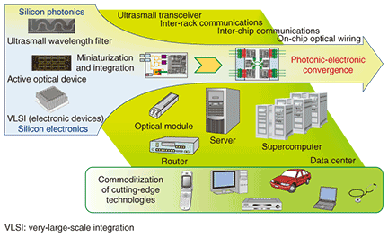
Efforts to apply silicon photonics to communications are described below. Current optical devices consist of optical fibers, wavelength filters, modulators, photodetectors, light-emitting diodes, and electronic control circuits. These devices are manufactured as separate components made of various different materials, and since they must be combined and installed as such, it has been difficult to lower costs. Features (1) and (2) above could solve this problem. Specifically, R&D is moving forward to achieve small low-cost optical devices by integrating silicon-based optical devices with optical devices made from (non-silicon) materials that can be handled during the LSI mass-production process. Progress is presently being made in technologies for fabricating optical devices and integrating them. On the other hand, silicon-based light-emitting devices are under development, and research on bonding and mounting lasers made of non-silicon materials is being performed in parallel. Besides communications, the outstanding features of silicon photonics are also being applied in the semiconductor industry with the aim of solving the problem of high power consumption in electronic circuits. At present, the use of multi-core central processing units (CPUs)—the brains of computers—is expanding as one way of controlling power consumption while maintaining the trend toward high-performance electronic circuits. In a multi-core scheme, a large number of signals must be transmitted at high speed, but when metallic wiring is used, limitations due to signal delays and increases in power consumption arise. To overcome these limitations, researchers are investigating optical interconnection technology based on wavelength division multiplexing by applying miniaturization (feature (1)) and optical/electronic integration (feature (3)). In addition, progress is being made in developing devices with diverse functions (feature (4)). 3. International R&D trendsForming optical circuits on silicon is not a recent idea—it was originally proposed by Richard Soref in the USA back in the 1990s [1]. However, achieving ultrasmall silicon-based optical circuits on the order of a few hundred nanometers required advances in fine processing technology for fabricating nanometer structures with high precision. From 2000 to 2005, research on silicon optical circuits escalated as process technology progressed and demands for solving the abovementioned problems with electronic circuits appeared. Intel showed that an optical source based on Raman scattering could be achieved in a silicon optical circuit. This drew attention to the idea of making low-cost transceivers by mounting all-optical devices on silicon. Since about 2005 or 2006, all research concerned with silicon optical devices and their integration technologies has been known as silicon photonics. At present, silicon photonics is being pursued in the USA, Europe, and Asia, with each region having its particular R&D focus. In the USA, many corporations and universities are researching and developing silicon photonics. MIT (Massachusetts Institute of Technology) maintains a silicon photonics technology roadmap to provide guidance for technology development. In its latest communication technology roadmap [2], target periods for technology development have been pushed forward five years. This roadmap indicates the increasing demand for silicon photonics technology and promotes the acceleration of technology development. Silicon photonics in the USA is viewed as a technology for achieving super-high-performance computer systems, and technology development there is moving forward as a national policy centered on the public DARPA (Defense Advanced Research Projects Agency) program. It has so far been shown that optical and electronic circuits can be formed on the same silicon substrate by using a silicon CMOS (complementary metal oxide semiconductor) process and that photonic-electronic convergence is feasible. These results have laid the foundation for a recent technology development program that aims to achieve a supercomputer on a Si substrate by constructing optical interconnections between CPUs in a multi-core configuration. In Europe, meanwhile, elemental technology development centered on public institutions like IMEC (Interuniversity Microelectronics Center) is making progress with an eye toward a wide range of applications, such as computers, communications, and sensors. A global silicon photonics foundry service has been established, and in recent years, many reports have been issued by universities and corporations concerning work done using this service, which demonstrates its effectiveness. In Japan, the emphasis is on basic R&D with the focus mainly on materials development at universities. In 2006, a national project was launched, and research on optical wiring for application to electronic circuit systems has already generated results. Elsewhere in Asia, IME (Institute of Microelectronics) in Singapore has launched a foundry service to support developments up to the commercialization level. In the above way, competition in silicon photonics R&D is intensifying throughout the world in a wide range of technical areas ranging from basic technologies to system development. 4. R&D at NTTNTT Microsystem Integration Laboratories has been researching and developing silicon photonics for communications since 2000. During this time, our efforts have focused on solving three major problems in applying silicon optical devices to optical communications. (1) In silicon wire waveguides, which are a few hundred nanometers in size, even slight irregularities on the waveguide surface will cause light to scatter, resulting in large propagation loss and light blockage. (2) Since the cross sectional area of a silicon wire waveguide is significantly smaller than that of an optical fiber core (only 1/1000), direct connection between an optical fiber and silicon optical circuits is difficult. (3) Even a slight difference in the horizontal and vertical shapes of a silicon wire waveguide will produce different results depending on the polarization state of the propagating light (polarization dependence). To solve problem (1), the most basic of these problems, NTT studied low-loss optical waveguide fabrication technology. This resulted in the development of nanometer processing technology applicable to optical waveguides and produced a silicon wire waveguide with the smallest loss ever achieved (about 1 dB/cm) [3]. To solve problem (2), NTT placed a proprietary reverse-tapered spot-size converter between the optical fiber and silicon waveguide, enabling connections with a low loss of 0.5 dB/point [4]. These two world-leading technologies made it possible to manufacture and accurately evaluate ultrasmall optical devices having wavelength filtering, modulation, and other functions. To solve problem (3), NTT studied polarization-independence technology and demonstrated a realistic ultrasmall polarization-diversity circuit capable of separating and rotating polarized waves and recombining them. Details of this technology are given in the second article of this Special Feature [5]. Currently, NTT is investigating technology for integrating optical and electronic circuits for silicon photonics. The key to integrating optical devices made of silicon and non-silicon materials on a silicon substrate is a method of integrating these devices while maintaining the performance of each individual device. As an example of such integration, the third article in this Special Feature [6] presents the results of integrating a germanium photodetector with silicon optical devices. To reduce power consumption in network optical devices by exploiting the material properties of silicon, NTT Photonics Laboratories is researching ways of embedding silicon wire waveguides into optical devices made of quartz. NTT currently uses quartz-based thermo-optic (TO) devices in the optical network. In these devices, the optical intensity and path are controlled by heating the quartz to change its refractive index. Since the temperature coefficient of the refractive-index of silicon is one order of magnitude higher than that of quartz, embedding a silicon waveguide in a quartz waveguide has yielded a TO device that can operate at lower power. Details are given in the fourth article in this Special Feature [7]. NTT Basic Research Laboratories (BRL) has also been engaged in silicon photonics research. Revolutionary devices, such as ultralow-power-driven optical memories and switches, have been investigated. These devices utilize slow light in waveguides or small cavities made of silicon photonic crystals. Details are given in the fifth article in this Special Issue [8]. Silicon photonics research at BRL is also active in the area of quantum cryptography, which is expected to achieve the ultimate security in communications. The aim here is to use a silicon wire waveguide to develop the quantum-entanglement light source needed to extend communication distances. Inside a silicon wire waveguide, a high optical density can be obtained and four-wave mixing—a nonlinear phenomenon—can be induced. Some of the photon pairs generated by four-wave mixing are in a quantum-entanglement state, which has the special property that when one of the photons of such a pair is measured, the state of the other photon also becomes known. This can be used to extend communication distances in quantum cryptography communication. More information about this research is given in the sixth article in this Special Feature [9]. In the above ways, silicon photonics R&D at NTT Laboratories is making steady progress toward devices that will revolutionize future communications. 5. Concluding remarksSilicon photonics and photonic-electronic convergence based on silicon photonics will have a ripple effect that should lead not only to improvements in optical devices and information appliances but also to flexible operation of networks and an overall drop in costs and power consumption. As shown in Fig. 3, cutting-edge technologies like those used in state-of-the-art supercomputers—which are being made possible by photonic-electronic convergence—are expected to be commoditized and incorporated into all kinds of electronic appliances. Through this process, photonic-electronic convergence has the potential to become the foundation of the advanced information society. NTT aims to contribute to society through the development of this technology.
References
|
||||||||||||||||||||||