|
|||||||||||||||||||||
|
|
|||||||||||||||||||||
       |
Special Feature: Silicon Photonic Technologies Leading the Way to a New Generation of Telecommunications Vol. 8, No. 2, pp. 11–16, Feb. 2010. https://doi.org/10.53829/ntr201002sf2 Polarization-independent Ultrasmall Silicon Photonic CircuitsAbstractThis article introduces polarization diversity technology that could solve the problem of polarization dependence in ultrasmall silicon photonic circuits, which is hindering their practical implementation. Polarization-manipulating devices fabricated using ultrafine nanoprocessing and thin-film-formation technologies should lead to inexpensive, low-power photonic devices for telecommunications use. 
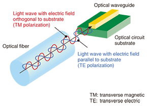
1. IntroductionThe propagation of light from an optical fiber toward an optical waveguide is schematically illustrated in Fig. 1. The electric field, which oscillates transversely to the propagation direction of the light, has two degrees of freedom—parallel and orthogonal—with respect to the optical circuit’s substrate. Since the magnetic field always oscillates perpendicular to the electric field, it is usually ignored in discussions and only the electric field is described. The direction of oscillation of the electric field is the polarization of the light waves. Since light waves propagating from an optical fiber may have various polarizations, the optical circuit receiving the signals should ideally have polarization-independent operating characteristics. For example, a wavelength filter, which is a key element of an optical circuit, should pass light waves of the same wavelength regardless of their polarization. In practice, however, waveguides in optical filters usually exhibit different propagation characteristics for different polarizations. This polarization dependence is quite large in ultrasmall silicon photonic circuits, which are promising owing to their ultrasmall size, low-power characteristics, and suitability for photonic-electronic convergence. Polarization dependence is a serious problem that is hindering practical applications of silicon photonic circuits.
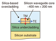
In this article, we first describe polarization dependence in ultrasmall silicon photonic circuits and then introduce polarization diversity technology as a solution to this problem. 2. Polarization dependencein ultrasmall silicon photonic circuitsAn ultrasmall silicon photonic circuit consists of silicon wire waveguides with the cross sectional structure shown in Fig. 2. The core of the waveguide is made of silicon, which is a material widely used in electronic circuits, and the cladding layers are made of silica-based materials. For infrared light with a wavelength of 1550 nm, which is widely used in telecommunications, the cross section of the core is extremely small: 400–500 nm wide and 200–300 nm high. This cross sectional area is about 1/1000 that of the silica waveguides used in conventional optical circuits. A curved waveguide can have an extremely small bending radius of a few micrometers, enabling the construction of very small, high-density optical circuits [1]. However, such a waveguide often exhibits very strong polarization dependence. Polarization dependence can be expressed in terms of the speed of the light wave propagating through the waveguide. For example, the phase velocity of 1550-nm light in a waveguide with a 460 nm × 200 nm core is 44% of the speed of light in a vacuum for polarization parallel to the substrate (transverse electric (TE) mode) and 62% for polarization orthogonal to the substrate (transverse magnetic (TM) mode). These two values are significantly different. Polarization dependence also exists for transmission loss and bending loss in the curved region.
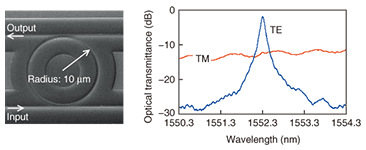
If optical waveguides have polarization-dependent characteristics, then the optical circuit containing them also has polarization-dependent characteristics. For example, a ring resonator with a radius of 10 μm, one of the simplest optical filters using a silicon wire waveguide, has the transmission characteristics shown in Fig. 3. As shown, the filter has excellent performance for TE polarization but is essentially ineffective for TM polarization, making it useless as a communications device.
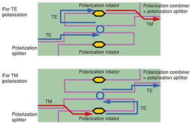
Although polarization dependence can be reduced by using a square core, which has symmetry in both the up/down and left/right directions, that is not a realistic solution. For example, in recent wavelength filters for wavelength-division-multiplexing (WDM) communications systems handling several tens of wavelengths, it would be necessary to keep the velocity difference between TE and TM polarizations to within 0.01%, which would require controlling the core shape to within 0.1 nm. However, even state-of-the-art silicon fabrication techniques are incapable of making such an ultrafine structure. Thus, instead of trying to eliminate the polarization dependence of waveguides, we devised an optical polarization diversity circuit based on a silicon waveguide. 3. Polarization diversity circuit for ultrasmall silicon photonic devicesThe configuration of our polarization diversity circuit is shown in Fig. 4 [2]. This circuit consists of polarization splitters, polarization rotators, and a ring-resonator wavelength filter as an example of a functional device. The incident light is initially separated into TE and TM polarization components by a polarization splitter. The TE-polarized light from the splitter is directly guided into the ring resonator, which passes only the desired wavelengths. The TM-polarized light from the splitter is guided first to a polarization rotator, where it is converted into TE-polarized light, and into the ring resonator from the opposite direction to that of the original TE-polarized light. Since the TM-polarized light from the splitter has been converted into TE-polarized light, the ring can also work as a wavelength filter for this light. Since the two output lights from the ring are guided in opposite directions, no interference occurs at this point. However, interference would eventually occur if these two TE-polarized lights were combined into one waveguide at the end. To avoid this interference, we arrange for one of the output lights from the ring to be converted into TM-polarized light by a rotator, and these two outputs are combined by a polarization splitter oriented in the reverse direction. A key feature of this polarization diversity scheme is that both the original polarization components use the same functional device, which presents exactly the same device characteristics to them both.
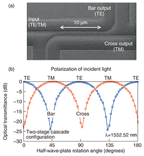
This polarization diversity circuit requires polarization splitters and rotators formed from silicon wire waveguides. We have succeeded in constructing these polarization-manipulation devices by using ultrafine nanoprocessing technology and thin-film-formation technology. A scanning electron micrograph of our polarization splitter—a simple 10-μm-long directional coupler—is shown in Fig. 5(a) [3]. In this coupler, the TM component of the incident light crosses over to the neighboring waveguide while the TE component continues forward in the incident waveguide. Thus, polarizations are separated into different outputs (cross and bar). The optical intensity measured at each output port while the polarization of the incident light was alternated TE→TM→TE→TM … is shown in Fig. 5(b). It can be seen here that the output-port intensity reversed as the input polarization changed from one type to the other. This experimental result clearly shows that the TE and TM components were output to their respective ports [3].
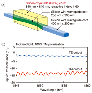
The structure of our polarization rotator is shown in Fig. 6(a) [4]. This device has an off-axis double-core structure consisting of a 200-nm-square silicon wire core and a second 840-nm-square silicon-oxynitride (SiON) core constructed on the silicon core. This asymmetric double-core waveguide structure can rotate the polarization of light. The output light power spectra when TM-polarized light was introduced into the 35-μm-long double-core structure are shown in Fig. 6(b). Although the input here was TM-polarized light, the main component at the output was TE-polarized light. The output intensity of TM-polarized light was less than 1/10 that of TE-polarized light [4]. In other words, TM-polarized light was converted into TE-polarized light.
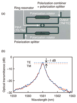
A micrograph of a polarization diversity circuit that we fabricated by combining these polarization splitters and rotators is shown in Fig. 7(a) [2]. Here, a ring resonator identical to the one in Fig. 3 is located in the center and surrounded by polarization splitters and rotators in the same configuration as in Fig. 4. The transmission characteristics of this ring-resonator wavelength filter with the polarization diversity circuit are shown in
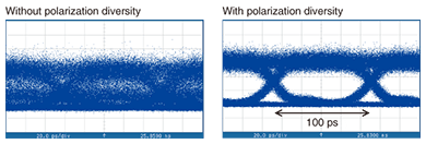
The output-signal eye patterns when a 10-Gbit/s modulated optical signal with random polarization was introduced into the ring resonator filter are shown in Fig. 8. Without polarization diversity, the main signal was disordered, but with the polarization diversity circuit, the signal showed well defined eye opening [2].
4. ConclusionPolarization diversity can solve the problem of polarization dependence in ultrasmall silicon photonic circuits. We believe this is a breakthrough technology toward practical applications of ultrasmall silicon photonic circuits. Looking forward, we plan to refine it and perform further studies with the aim of making polarization-independent technologies suitable for various kinds of optical devices. Our objective is to contribute to the provision of ultrasmall, low-power telecommunications modules featuring photonic-electronic convergence on an ultrasmall silicon photonic circuit platform. References
|
||||||||||||||||||||