|
|||||||||||||||||||||||||
|
|
|||||||||||||||||||||||||
       |
Special Feature: Silicon Photonic Technologies Leading the Way to a New Generation of Telecommunications Vol. 8, No. 2, pp. 17–22, Feb. 2010. https://doi.org/10.53829/ntr201002sf3 Ultrasmall Silicon Photonic Devices and Integration Technology Toward Photonic-electronic ConvergenceAbstractThis article introduces the current status of silicon photonic device integration technology using, as an example, the monolithic integration of a silicon-wire-waveguide variable optical attenuator and a germanium photodetector, which are devices that we have developed with photonic-electronic convergence in mind. 
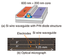
1. IntroductionWith the introduction of broadband optical networks in homes and offices, users can now exchange video and other types of large content. However, if optical services are to expand even further, communication networks will have to be made faster and less power hungry and the cost of services will have to be reduced. To this end, the market demand is for higher performance and lower cost in various types of devices used for optical communications. Like modern electronic devices, for which the silicon large-scale integrated circuit (LSI) is a key example, optical communications devices will have to offer high performance and low cost simultaneously if ones for various functions are to be densely integrated on the same chip. However, the extent to which existing optical devices can be integrated on the same chip is limited because various different materials are used to form individual devices according to the intended function. In addition, the materials, sizes, and fabrication processes for optical devices are different from those for electronic circuits, making the monolithic integration of optical and electronic devices difficult. Silicon photonics is a promising technology that could lead to the development of optical devices whose materials and dimensions are compatible with Si LSI processes. It should enable us to monolithically integrate not only optical devices but also the combination of optical and electronic devices on the same Si substrate. This should drive the provision of low-cost, high-performance devices through photonic-electronic convergence and integration and Si-based mass-production manufacturing techniques [1]. Researchers have only recently begun to investigate the on-chip convergence and integration of optical and electronic devices, and there are many problems that need to be solved. In this article, we first introduce two devices that we have developed with photonic-electronic convergence and integration in mind: 1) a variable optical attenuator (VOA) that combines a Si wire waveguide and a PIN (positive/intrinsic/negative) diode and 2) a Ge photodetector (PD) that couples with a Si wire waveguide. We then describe the present status of monolithic integration technology for optical devices on a Si substrate using the integration of these two devices as an example. 2. VOA based on Si wire waveguide with PIN diode structureOptical communications requires devices that can alter optical intensity. If a Si semiconductor is used as the core of an optical waveguide, a diode structure can be incorporated within the waveguide, which means that an optical modulator device for altering the intensity of light can be achieved by having current flow through the core. Our VOA consists of a Si wire waveguide with a PIN diode structure, as shown in Fig. 1 [2]. The waveguide has an ultrasmall rib-type structure with a core cross-sectional size of 600 nm × 200 nm and a slab thickness of 100 nm. The slab areas on both sides of the core are injected with impurities to create very heavily doped positive (p+) and negative (n+) semiconductor regions. This structure is achieved through a combination of nanoprocessing technology used for ultrasmall Si photonic waveguides and ion-injection and impurity-diffusion techniques used in LSI fabrication [3]. A forward bias voltage applied to the lateral PIN diode forces free carriers (electrons and holes) into the core (intrinsic layer of this PIN diode). The injected free carriers then absorb light, which results in optical attenuation.
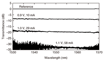
The transmission spectra measured at the VOA output port when the amount of current injected into the VOA was varied are shown in Fig. 2. These results show that the optical intensity (transmittance) attenuated as the injection current was increased and could be controlled within an attenuation range of 30 dB. One feature of this VOA is that the spectra are flat regardless of the wavelength, which means that a fixed level of optical attenuation can be obtained over a wide wavelength region.
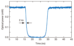
Another feature of the Si-wire-waveguide VOA is that its small core enables carriers to be injected into and removed from the core in a relatively short time, which leads to high-speed operation. The optical response obtained when a rectangular electronic pulse with a width of 15 ns was applied to this VOA is shown in Fig. 3. This result shows that attaching the PIN diode structure to a Si wire waveguide enables rapid control of the intensity of the propagating light. We are also developing optical modulators operating at speeds above 1 GHz by incorporating PIN structures into Si-wire-waveguide Mach-Zehnder interferometers and ring resonators.
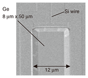
3. Ge PD coupled with a Si wire waveguideA PD is essential for converting optical signals into electrical signals. Current optical communications systems use PDs made of compound semiconductor material. In Si photonics, however, PDs made from Ge are preferred because Ge has a high affinity with Si and can be formed monolithically on a Si waveguide core. Ge PDs are expected to allow compact low-cost integration even for a multichannel configuration. With the aim of achieving a Ge PD coupled with a Si wire waveguide, we developed, in collaboration with the University of Tokyo, a process for selectively growing a very small Ge film a few micrometers by a few tens of micrometers in size on a Si surface connected to a Si wire waveguide. A scanning electron micrograph of such a Ge film formed on a Si surface is shown in Fig. 4. It demonstrates that a low-defect Ge film can be formed selectively at one end of a waveguide. After the Ge film was grown on a p-type Si region, an n-type Ge region was formed by implanting ions into the upper section of the Ge to obtain a Ge PD with a vertical PIN structure [4].
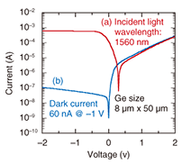
Ge has a refractive index of 4.0, which is higher than that of Si, so light propagating through the Si core is absorbed by the Ge, resulting in the generation of carriers in it. The accumulated carriers are then extracted as a photocurrent. The results of an evaluation of the characteristics of a Ge PD connected to a Si wire waveguide are shown in Fig. 5. The upper and lower curves show current-voltage characteristics with and without incident light on the waveguide. The current when a reverse voltage was applied is the photocurrent. Without incident light, the current (i.e., dark current) was 60 nA at –1 V, which is a sufficiently small value. The photocurrent increased significantly when light was incident and a favorable responsivity value of 0.8 A/W was obtained for the PD. The PD operated at speeds of 1 GHz and above.
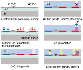
4. Monolithic integration of Si VOA and Ge PDIn attempts to monolithically integrate two devices, it is important that the fabrication process of one device does not interfere with that of the other. The fabrication process flow for monolithically integrating a Si VOA and a Ge PD is shown in Fig. 6. Here, device fabrication requires various processes such as film growth, patterning, etching, implantation, washing, and thermal processing. During these processes, the substrate is subjected to plasma, ions, heat, and chemicals. Thus, depending on the fabrication sequence, one device is susceptible to damage during the fabrication of the other device. Giving due consideration to the characteristics of each process and the resistance of each device, we chose a process sequence that achieves monolithic integration of the Si VOA and Ge PD without adversely affecting either device [5].
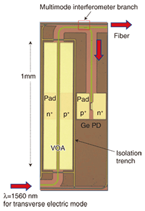
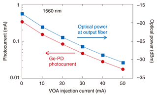
An optical micrograph of the fabricated integrated device is shown in Fig. 7. One branch of a multimode interferometer was placed between the Si VOA and Ge PD to route light to the outside for device evaluation. Evaluation results for the optical detection of Si-VOA-modulated light by the Ge PD connected to the Si wire waveguide are shown in Fig. 8. The photocurrent at the detector agrees well with the change in optical power. These results demonstrate that a Ge PD can correctly detect the attenuation of optical intensity produced by a VOA through the injection of carriers. They also show that these monolithically fabricated devices can operate well synchronously.
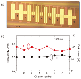
Multichannel integration of devices is necessary for optical wavelength division multiplexing (WDM) to be used in communications networks. Because Si-photonic devices are small and can be integrated, the integration of multiple devices for multichannel purposes is relatively straightforward. An optical micrograph of a chip integrating Si VOAs and Ge PDs in an array of eight device pairs is shown in Fig 9, which also shows the results of evaluations of the dark current and responsivity of each Ge PD in this array. These results show that nearly uniform characteristics were obtained for all eight PDs and that multichannel integration if feasible. We have also been successful in integrating VOAs and PDs for 40-channel use in a small region: 4 mm × 12 mm.
5. ConclusionBasic photonic devices working at a practical level are now emerging thanks to the rapid advances made in Si photonics over the last few years. The outlook for the integration of these devices is also good. However, researchers have only just begun to investigate the convergence and integration of optical and electronic devices—an area in which the excellent features of Si photonics should be most effective—and there are still many problems to be addressed. Looking forward, we intend to devote our efforts to achieving Si-based photonic-electronic convergence and thereby contribute to the development of high-performance, low-cost communications networks. AcknowledgmentsThe Ge detector was a product of joint research with the Wada Laboratory, University of Tokyo, and the Ge film-growth process was carried out at the University of Tokyo. We would like to thank all concerned for their assistance in this research. References
|
||||||||||||||||||||||||