|
|||||||||||||||||||||||||||||
|
|
|||||||||||||||||||||||||||||
       |
Special Feature: Silicon Photonic Technologies Leading the Way to a New Generation of Telecommunications Vol. 8, No. 2, pp. 33–38, Feb. 2010. https://doi.org/10.53829/ntr201002sf6 Entanglement Generation Using Silicon Wire WaveguideAbstractGenerating high-purity entangled photon pairs is an important step toward quantum information processing using photons. In this article, we describe the world’s first ever experiment on generating entanglement using a spontaneous parametric process in a silicon wire waveguide. 
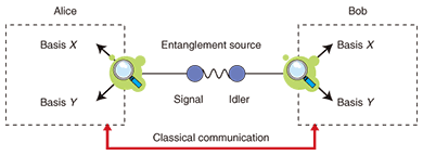
1. IntroductionIn recent years, information processing using the principles of quantum mechanics, including quantum cryptography and quantum computation, has been studied intensively. Quantum entanglement is an essential resource for quantum information processing. In particular, an entangled photon pair [1], which is an entangled state of photons, has been investigated as a way of distributing entanglement over long distances. In this article, we describe the world’s first ever experiment on generating entangled photon pairs using a silicon wire waveguide [2], [3]. 2. Time-bin-entangled photon pairAn entangled photon pair is a state where two photons show a correlation that cannot be explained by the classical theory. For example, a polarization-entangled photon pair is a state in which the polarization state of each photon is not fixed, but the relationship between the polarization states of the two photons is predetermined [1]. On the other hand, a time-bin-entangled state is based on a time-bin qubit, which is a superposition of two quantum states of photons in two distinguishable temporal positions. In a similar manner to that for polarization-entangled photons, we can describe a time-bin-entangled photon pair as being a state in which the temporal position of each photon is not fixed, but the two photons are always found in the same time slot. Here, we call the photons of an entangled pair the signal photon and the idler photon. The quantum state of a time-bin-entangled photon pair is given by  where In fact, we can get the situation in which the temporal position of each photon is not fixed, but the two photons are always found in the same time slot using two classically correlated photons. However, with classically correlated photons, the correlation between the measurement outcomes vanishes if we measure the photons using a basis that is not orthogonal to the original basis (for example, a polarization measurement that discriminates ±45° linear polarization is non-orthogonal to a horizontal/vertical polarization measurement). An example of a measurement that is non-orthogonal to the measurement that discriminates the states  Using the states defined in Eq. (2), we can rewrite Eq. (1) as  This equation clearly shows that the correlation of the measurement outcomes for two photons is still preserved even when we use a non-orthogonal measurement basis. This is a very important characteristic of an entangled photon pair, which cannot be achieved using two classically correlated photons. 3. Quantum key distribution using entangled photon pairsWe can implement various quantum information tasks using the peculiar characteristics of entangled photons explained in the previous section. Here, as an example of such a quantum information task, we describe quantum key distribution (QKD), where a secret key for cryptography is distributed between two distant parties. The configuration, in which a key is established between Alice and Bob, is shown in Fig. 1. We prepare many entangled pairs and send the signal and idler photons to Alice and Bob, respectively, over conventional optical transmission lines such as optical fibers. Both Alice and Bob are equipped with two measurement setups that correspond to two non-orthogonal measurements. Here, we call the measurement that discriminate states
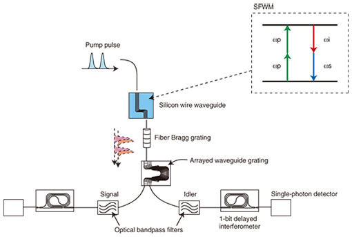
It is fundamentally impossible to eavesdrop on the key created by QKD, so we can achieve unconditionally secure communication by using QKD. Intuitively, the security originates from the fact that any two classically correlated photons cannot fully mimic the characteristics of entangled photon pairs (of course, very careful treatment is required to prove the unconditional security of any QKD protocol). Currently, secret communication based on QKD is expected to provide ultimate network security for future communication networks. 4. Entanglement generation using silicon wire waveguideWe generated 1.5-μm-band entangled photon pairs using a silicon wire waveguide [4]. A silicon wire waveguide is a single-mode, single-crystal silicon waveguide whose core diameter is typically 400 nm wide and 200 nm thick. Thanks to this extremely small core, the optical power density in the waveguide is very high, and as a result, we can observe a huge nonlinear effect. The nonlinear coefficient of the waveguide used in our experiment was five orders of magnitude higher than that of a conventional silica fiber. Since silicon is an inversion symmetric material, we can use it for a third-order nonlinearity experiment. In the present experiment, we generated time-bin-entangled photon pairs by spontaneous four-wave mixing (SFWM), which is one of the third-order nonlinear effects. When we input a 1.5-μm pump light whose angular frequency is given by ωp into a silicon wire waveguide, we can generate a photon pair with angular frequencies of ωs and ωi through SFWM. The following relationship exists between ωp, ωs, and ωi.  This equation implies that two pump photons are annihilated and a signal-idler photon pair is created. Since the two photons are created simultaneously, we can generate a temporally correlated photon pair state, in which two photons are always observed in the same time slot (for example, Thus, we can obtain a temporally correlated state, but it is still not entangled, as shown by Eq. (1). To generate an entangled state, we use a double pulse as a pump. Here, the phase difference between two pump pulses is fixed, so the first and second pulses probabilistically create pair states This technique enables us to make a simple, stable entanglement source in the 1.5-μm band. In addition, the use of a silicon waveguide enables us to avoid noise photons caused by spontaneous Raman scattering, which has been a serious problem for entanglement sources based on SFWM in an optical fiber [5]. 5. ExperimentWe generated time-bin-entangled photon pairs using the setup shown in Fig. 2. We injected 1551.1-nm double pulses into a silicon wire waveguide. The waveguide used in the experiment was 460 nm wide, 220 nm thick, and 1 cm long, and the waveguide loss was approximately 1 dB. The SFWM process inside the waveguide generated the quantum state shown by Eq. (1). The photons generated from the waveguide were first passed through a fiber Bragg grating to suppress the pump photons and input into an arrayed waveguide grating to separate the signal and idler photons. The wavelengths of the signal and idler photons were 1547.9 and 1554.3 nm, respectively. Each photon was passed through an optical bandpass filter to further suppress the residual pump photons, and then launched into a 1-bit delayed interferometer, which is an unbalanced Mach-Zehnder interferometer whose path difference corresponds to the time interval between the two pump pulses. The photons output from the interferometers were detected by single-photon detectors.
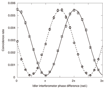
When a photon whose state spans two time slots is launched into the 1-bit delayed interferometer, the single-photon detector connected to the interferometer output could detect the photon in any one of three time slots. Photon detection in the second time slot means that the input state is projected to a state given by  where φy is the phase difference induced in the interferometer. Thus, we can implement measurement bases that correspond to To confirm the generation of time-bin entanglement, we set the phase difference of the signal interferometer to 0 (φs = 0) and observed the coincidence counts of two photons as a function of idler interferometer phase difference φi. The results are shown by squares in Fig. 3. We observed a clear sinusoidal modulation of the coincidence counts, which indicates that the measurement results for the signal and idler photons were correlated. The waveform had peak values at φi = 2 n π (n: integer). This means that the coincidence rate was maximum when the signal and idler photons were both projected to
We then set φs = –π/2, which let us implement a non-orthogonal basis for measuring signal photons, and measured the coincidence fringe. The results (circles in Fig. 3) clearly show that the measurement results for two photons were again correlated even with the non-orthogonal basis. Thus, we successfully confirmed the generation of an entangled state. The visibilities of the coincidence fringes were 96.3% (φs = 0) and 95.2% (φs = –π/2), implying that we obtained high-purity entanglement in the 1.5-μm band. 6. ConclusionNTT has performed the world’s first ever entanglement generation experiment using a silicon wire waveguide. This technique is expected to provide a practical and high-purity entanglement source in the 1.5-μm telecommunication band, which will enable us to achieve quantum communication over optical fibers in the future. References
|
||||||||||||||||||||||||||||
 x
x y denotes the quantum state where there is a photon in the xth time slot and in mode y (=s: signal, i: idler).