|
|||||||||||||||||||||
|
|
|||||||||||||||||||||
       |
Special Feature: Trends and Business Prospects for Human-area Networking Technology––Connecting People, Objects, and Networks Vol. 8, No. 3, pp. 7–12, Mar. 2010. https://doi.org/10.53829/ntr201003sf2 LSIs for an Advanced Compact Electric-field Communication ModuleAbstractIn this article, we describe a digital LSI (large-scale integrated circuit) and an analog LSI designed for an advanced compact communication module based on near-field communication using the human body as the transmission path. The two key techniques that ensure stable communications are high-efficiency AC (alternating current) electric-field induction and ambient noise reduction. Applications of the technology are also described. 
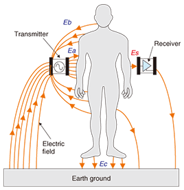
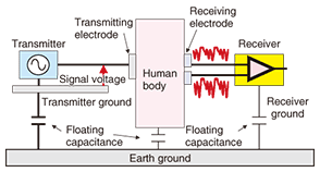
1. IntroductionWith the rise in interest in ubiquitous computing over the last twenty years, there has been active development of technology for communicating over relatively short distances. Recently, there has been progress toward practical technology for extremely short-distance wireless communication using the human body as the transmission path. The main advantage of this is that communication and operation can be linked. Connection to a network can be achieved through natural actions such as touching or taking a step, so it offers an intuitive interface with computer hardware. In our group, we are studying a method that uses an alternating current (AC) electric field and are conducting research and development on human-body near-field communication technology. For this technology to come into wide personal use, it must be compact and inexpensive, so the electronic components should be fabricated as LSI (large-scale integration) chips. In this article, after briefly reviewing the principle of human-body near-field communication, we describe the LSIs we have developed and an evaluation of a prototype terminal implementing them. 2. Human-body near-field communication technologyBroadly speaking, there are two approaches to using the human body as the transmission path for communication: the electric-field type and the electric-current type. The electric-field approach was first verified by Zimmerman of MIT [1] and then improved in terms of speed through work by NTT using optical sensors in the receiver to achieve a transfer rate of 10 Mbit/s [2]. The electric-current approach, on the other hand, is used in body fat measurement, which uses a very weak current flow, and there have also been reports of application to retail scales for weighing products like meat [3]. This approach requires a flow of current in the human body, so metal electrodes must be in contact with the body. Therefore, applications are limited to devices in direct contact with the skin, such as wristwatches with a built-in body fat measuring function. The electric-field approach allows communication without direct skin contact, such as from a pocket or neck strap, so it allows a wider range of applications and greater convenience. For these reasons, we have focused on the electric-field approach and developed it to a practical level as RedTacton [4], [5]. A model of electric-field communication is illustrated in Fig. 1. We denote the electric-field signal generated in the human body from the signal electrodes of the transmitter as Ea. This signal is returned to the transmitter via the circuit’s ground as electric-field signal component Eb. If the person is connected to the earth ground (e.g., via the floor of a building), electric-field signal component Ec escapes to the earth ground. Eb and Ec are very large, so the signal that reaches the receiver is greatly attenuated. Accordingly, the receiver must be able to detect very weak electrical-field signal components with high sensitivity. The signal path model for when the receiver shown in Fig. 1 is placed close to the earth ground is shown in Fig. 2. The receiver’s signal electrodes are susceptible to electromagnetic noise from the environment and its ground electrodes are susceptible to noise introduced via floating capacitance with the earth ground. Therefore, a mechanism to prevent that noise from causing receiver malfunctions is required. Specifically, both filters for removing noise components and differential detection for suppressing ambient noise are needed.
3. LSIs for electric-field communicationAn LSI to be used in human-body near-field communication must:
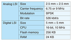
We have developed an analog LSI and a digital LSI that meet these requirements. The main specifications are given in Table 1.
3.1 Analog LSISince the receiver is susceptible to the effects of noise from the environment when the human body is used as a transmission path, we chose binary phase shift keying (BPSK) as the synchronization detection method because it provides high noise tolerance. The carrier frequency can be selected as either 6.75 or 9 MHz and the bit rate is about 500 kbit/s. The chip is 2.5 mm × 2.5 mm, and compact mounting is achieved by using wafer-level packaging. The chip configuration is shown in Fig. 3. The receiver can switch the data signal demodulation sensitivity and carrier signal detection sensitivity levels according to the electric-field signal strength. It also has a filtering function for digitally detecting the carrier signal in order to suppress ambient noise.
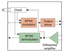
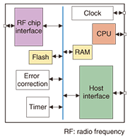
3.2 Digital LSIThe configuration of the digital LSI is shown in Fig. 4. We designed the digital chip to provide the same functions as an ordinary IC card. It has a 16-bit central processing unit (CPU) that operates at 10 MHz, a 256-KB Flash memory for storing application software and a 24-KB random access memory (RAM), and a connector for an external 32-KB electrically erasable programmable read-only memory (E2PROM) for IC card data. It measures 5 mm × 5 mm and, like the analog LSI, uses wafer-level packaging for compact mounting. Since portable devices are battery driven, LSI chips designed to be mounted on portable devices must have low power consumption. This digital LSI chip is designed for low power consumption and can be used in a terminal powered by a coin battery.
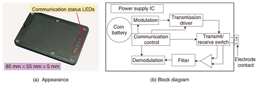
4. Terminal prototype and communication experiments4.1 Card terminalA block diagram and photograph of the card terminal are shown in Fig. 5. This terminal comprises the analog LSI, the digital LSI, an E2PROM, an oscillator, a power-supply IC, a coin battery (2.5 V), and electrodes. The front has light emitting diodes (LEDs) to indicate the communication state. The terminal measures 85 mm × 55 mm × 5 mm. The E2PROM stores various evaluation data for later analysis.
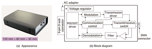
4.2 Embedded terminalA block diagram and photograph of an embedded terminal (terminal embedded in the environment) are shown in Fig. 6. This terminal comprises the analog LSI, the digital LSI, an E2PROM, an oscillator, an RS232C driver, a power-supply IC, and a transmission driver. It measures 120 mm × 80 mm × 30 mm. The power supply is 5 V and a 9-pin D-sub RS232C interface enables connection to external devices. The transmitting and receiving electrodes are connected to the terminal’s SMA connector via a coaxial cable.
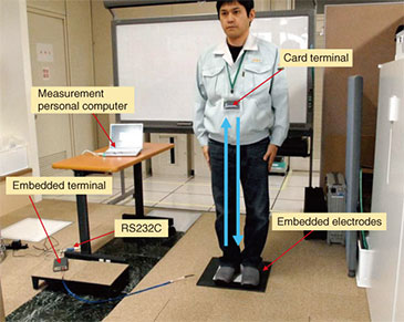
4.3 Evaluation resultsWe tested the communication between the card terminal placed on a person’s neck strap and an embedded terminal (Fig. 7). We used a communication evaluation program to separately test three communication conditions: 1) card terminal to embedded terminal, 2) embedded terminal to card terminal, and 3) card terminal to embedded terminal to card terminal.
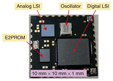
In the evaluation of two-way communication, a data packet containing a specified ID was transmitted from the embedded terminal, received and returned by the card terminal, and received again by the embedded terminal. The evaluation results for a transmission interval of 100 ms confirmed a packet success rate of 100%. If this evaluation system is combined with application software, it will be possible to implement various demonstration systems in which a person carrying a card terminal can unlock doors and activate entry control devices, maintain the security of printed materials when using printers and copiers, and lock and unlock cabinets, and so on, all by simply stepping on electrodes in the floor. 4.4 Compact moduleA communication module containing one analog LSI and one digital LSI, an E2PROM, and an oscillator can be implemented as an ultrasmall (10 mm × 10 mm) package (Fig. 8). This package can be mounted on the circuit boards of various devices by ordinary reflow mounting, which enables a wide range of applications.
5. Future developmentA more compact communication module would allow a greater variety of terminal types, including smart keys, wristwatches, and cell phones. Diversification into medical care giving and treatment, payment settlement, and other such services in addition to security applications will probably require greater functional flexibility through the use of rewritable firmware and faster LSIs to handle more data. Among future goals, one we are working toward is power consumption low enough to enable terminals to be powered by the tiny amount of electrical power generated by the human body (batteryless terminals). References
|
||||||||||||||||||||