|
|||||||||||||||||||||||||||||||||||
|
|
|||||||||||||||||||||||||||||||||||
       |
Letters Vol. 8, No. 8, pp. 44–51, Aug. 2010. https://doi.org/10.53829/ntr201008le2 Uncooled Operation of 10-/40-Gbit/s 1.55-μm Electroabsorption Modulator Integrated with Distributed Feedback LaserAbstractWe have developed two types of 1.55-µm-wavelength electroabsorption modulator integrated with a distributed feedback laser diode by using InGaAlAs material. One has a twin waveguide structure, which has the advantage of a simple fabrication process. Its output power reached 4 mW at 85°C. The other has a butt-joint structure, which has the advantage of design flexibility. Its measured power penalties were less than 2 dB after 10-Gbit/s 80-km single-mode-fiber transmission in the range from –25 to 100°C and 40-Gbit/s 2-km single-mode-fiber transmission from –15 to 80°C. 
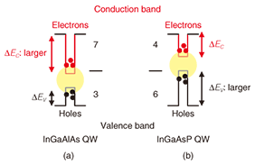
1. IntroductionThe recent increase in data and Internet traffic has required low-power-consumption and low-cost optical light sources for optical network systems. In an optical network system such as the 10-Gbit/s intermediate-reach (40 km), 10-Gbit/s long-reach (80 km), and 40-Gbit/s very-short-reach (2 km) categories, electroabsorption modulators integrated with distributed feedback laser diodes (EMLs) have been used as the optical light sources. Commercialized EMLs are cooled or semi-cooled with Peltier devices, which consume most of their power, so Peltier-device-free (uncooled) operation is an effective way to reduce the power consumption and fabrication cost of optical light sources, besides eliminating the cost of the Peltier device itself. However, uncooled EML operation presents challenges. At a high operating temperature, it is difficult to keep sufficient laser diode (LD) output power. On the other hand, at a low operating temperature, it is hard to obtain a sufficient extinction ratio because wavelength detuning (Δλ) between the lasing wav+elength (λDFB) and absorption peak of an electroabsorption modulator (EAM) multiple quantum well (MQW) becomes large, which leads to a decrease in absorption efficiency. Wide-temperature-range operation of 10- and 40-Gbit/s EMLs using InGaAlAs material has recently been demonstrated for both an LD MQW and an EAM MQW [1]–[4]. Schematic band diagrams of InGaAlAs- and InGaAsP-based quantum wells (QWs) are shown in Fig. 1. The ratio of conduction band offset (ΔEc) to valence band offset (ΔEv) is about 7:3 for InGaAlAs compared with 4:6 for InGaAsP [5]. At a high operating temperature, electrons and holes generally overflow from the LD MQW. Because the effective mass of an electron is smaller than that of a hole, the overflow of electrons mainly causes a decrease in LD output power. InGa-AlAs provides a larger ΔEc, which leads to stronger electron confinement. For these reasons, InGaAlAs material has temperature-tolerant characteristics. Moreover, the strong electron confinement also leads to greater oscillator strength for an exciton, which causes the larger extinction ratio.
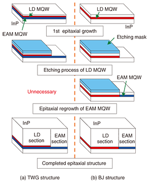
Some approaches that use InGaAlAs material to achieve uncooled operation of EMLs have been demonstrated. EMLs with the same layer structures for LDs and EAMs have been reported [6], [7]. This identical-layer structure makes it possible to omit EAM MQW epitaxial regrowth. A twin waveguide (TWG) structure approach for reducing the insertion loss of the EAM section to less than that of the identical-layer structure has also been described [1], [8]. A selective area growth technique that also enables the epitaxial regrowth process to be omitted has also been reported [9]. These structures focused on decreasing the number of epitaxial regrowth steps in the fabrication process, but one structure for which the focus is device design is the butt-joint (BJ) structure [2], [10]. The BJ structure lets us design the LD and EAM independently, so we can simultaneously have an LD designed for high output power at a high operating temperature and an EAM designed for a high extinction ratio at a low operating temperature. The most commonly used method of driving EMLs over a wide temperature range is the voltage-offset method [1], which changes the EAM bias voltage (Vb) while varying the operating temperature with a constant modulation voltage swing (Vpp). NTT Photonics Laboratories has developed a technology for fabricating InGaAlAs EMLs. In this article, we describe two types of InGaAlAs EMLs for the communication wavelength of 1.55 µm. One is a TWG-based EML and the other is a BJ-based EML. Section 2 explains their fabrication processes. Sections 3 and 4 describe the characteristics of the TWG- and BJ-based EMLs, respectively. The BJ-based EML’s 10- and 40-Gbit/s characteristics over a wide temperature range are also described in section 4. Finally, section 5 concludes with a short summary of the main points. 2. Device fabricationThe epitaxial growth processes for the TWG and BJ structures are schematically shown in Fig. 2. For the TWG structure, EAM and LD MQWs were grown on an n-InP substrate by metalorganic vapor-phase epitaxy (MOVPE). On the other hand, for the BJ structure, only the LD MQW was grown by MOVPE. In the etching process for the LD MQW, the LD MQW of the EAM section of both structures was removed by wet-chemical etching. Then, for the BJ structure, the EAM MQW was butt-joined to the LD MQW. The advantage of the TWG structure is that the EAM MQW regrowth process can be omitted. After removal of the etching mask, p-InP cladding layers were regrown on the LD and EAM MQWs for both structures. As can be seen in Fig. 2(a), in the TWG structure, the EAM MQW exists under the LD MQW, so Δλ of the TWG structure needs to be designed to be larger than that of the BJ structure. The advantage of the BJ structure is design flexibility for Δλ.
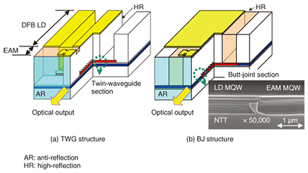
Schematic diagrams of the fabricated TWG- and BJ-based EMLs and a cross sectional scanning electron microscope image of the BJ section are shown in Fig. 3. After the epitaxial regrowth of the p-InP cladding layer, a ridge waveguide structure was fabricated by standard dry etching and wet chemical etching for both structures. After ridge waveguide formation, the entire structure was passivated and planarized with benzocyclobutene to reduce the pad capacitance. The next step involves formation of p-type contact pads on the LD and EAM sections. After thinning and cleaving of the wafer, the LD and EAM facets were high-reflection and anti-reflection coated. Finally, each device was mounted p-side up on an AlN heatsink and packaged in a conventional butterfly package [4].
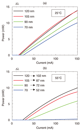
3. Twin waveguide structureIn this section, we describe the design of the TWG-based EML and its characteristics [8]. As shown in Fig. 3(a), the LD and EAM MQWs were stacked vertically, and only the LD MQW of the EAM section was removed to reduce the waveguide loss of the EAM section. The device consists of a 450-μm-long distributed feedback (DFB) LD, a 50-μm-long electrical isolation region, and a 200-μm-long EAM. The light emitted from the LD section is transferred to the isolation region and then to the EAM section. The key to achieving the wide-temperature-range operation of the TWG-based EML is to set Δλ to give sufficient LD output power at a high operating temperature. The Δλ dependence of the output power at 25 and 55°C is shown in Fig. 4. The Δλ values were 120, 105, 90, 70 nm at 25°C (a) and 102, 87, 72, 52 nm at 55°C (b) because the temperature sensitivity of λDFB and the absorption peak of the EA MQW are about 0.11 and 0.7 nm/°C, respectively. As indicated in Fig. 4(b), the output power at 55°C for Δλ of 102 nm reached 10 mW. From this basic experiment, we set Δλ to more than 120 nm at 25°C.
The temperature dependence of the output power is shown in Fig. 5 for (a) the DFB LD without the EAM MQW and (b) the TWG-based EML with Δλ of 120 nm at 25°C. The output power of the DFB LD was 14 mW at 85°C. On the other hand, the output power of the TWG-based EML at 85°C reached 4 mW. This result shows that the TWG-based EML has the potential to be a candidate for an uncooled light source.
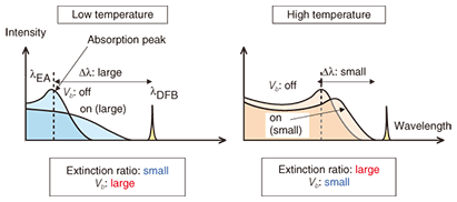
4. Butt-joint structureIn this section, we describe the design and characteristics of the BJ-based EMLs [10]. As shown in Fig. 5(a), higher output power can be obtained if there is no EAM MQW under the LD MQW. This can also provide sufficient output power with lower LD injection current (ILD) and it is suitable for reducing the power consumption of the light source. Qualitative diagrams of the relationship among Δλ, operating temperature, and Vb are shown in Fig. 6. At a low operating temperature, Δλ is large, so a larger Vb is required for EAM operation. In addition, the large Vb lowers the intensity of the absorption peak, which leads to a decrease in the extinction ratio. At a high temperature, Δλ becomes small. And the smaller Vb can give a sufficient extinction ratio because the intensity of the absorption peak does not become small when Vb is large. For the wide-temperature-range operation of EMLs, a sufficiently large extinction ratio and a sufficiently small Vb must be achieved simultaneously. We focused on EMLs operating from below 0°C to 100°C because the temperature range of an uncooled light source such as a directly modulated laser diode in this range has been reported [11]. We designed Δλ to be 60 nm at 100°C since Vb at 100°C is equal to Vb of conventional EMLs.
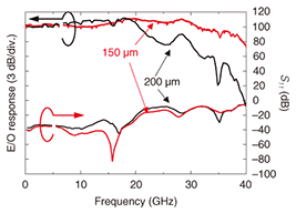
We then chose the EAM lengths for 10- and 40-Gbit/s operation. The limit on the operating speed depends on both the capacitance of the EAM and the characteristics of the radio-frequency (RF) transmission line to the EAM. To operate the EAM at high speed, we used an impedance-matched microstrip transmission line to supply the electrical signal to the EAM. The EAM length dependences of the small-signal electrical-to-optical (E/O) response and electrical return loss (S11) are shown in Fig. 7. S11 remained below –15 dB up to 20 GHz, which indicates that the RF return loss of the RF transmission line including the EAM was suppressed sufficiently for EAM lengths shorter than 200 μm. On the other hand, the E/O 3-dB-down bandwidth (f3dB) showed EAM-length dependence. These results mean that the capacitance of the EAM influences the E/O f3dB. The total EAM capacitance was determined by summing the capacitances of the metal pad and waveguide sections. The capacitance of the metal pad section was relatively small because the metal pad was fabricated on benzocyclobutene, which has a low relative permittivity (εr) of 2.8. The smaller capacitance of the 150-μm-long EAM gave E/O f3dB of 39 GHz. The 200-μm-long EAM gave E/O f3dB of 25 GHz. Therefore, we set the EAM lengths to 150 μm for 40-Gbit/s operation and 200 μm for 10-Gbit/s operation.
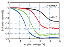
The device consists of a 450-μm-long DFB LD, a 50-μm-long electrical isolation region, and an EAM. Static extinction ratio (SER) characteristics of the 200-μm-long EAM at various operating temperatures from –25 to 100°C are plotted in Fig. 8. By designing Δλ and the EAM MQW carefully, we obtained an SER of over 14 dB at all operating temperatures. This result indicates that sufficient SER was obtained even at –25°C, which is a severe condition due to the larger Δλ.
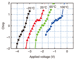
We measured the chirp according to a previously described procedure [12]. The measured chirp of the 200-μm-long EAM from –25°C to 100°C is shown in Fig. 9. As the operating temperature increased, the chirp shifted to a lower voltage due to the decrease in Δλ. We set Vb to obtain a negative chirp, but a larger Vb resulted in less output power, so there is a trade-off relationship between the output power and chirp. Measured chirp values were –1.2, –0.45, and –1.3 when Vb was set to –3.8, –2.9, and –1.3 V for –25, 25, and 100°C, respectively.
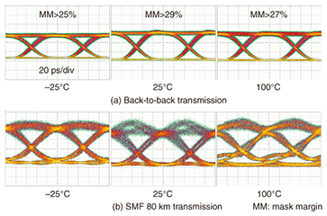
We used this device to perform a single-mode-fiber (SMF) transmission experiment. We used a 9.95-Gbit/s, non-return-to-zero (NRZ), 231–1 pseudorandom bit stream (PRBS) while maintaining a constant Vpp of 2.5 V at all temperatures. The filtered eye diagrams obtained when only Vb was adjusted at all temperatures are shown in Fig. 10. The upper and lower images are for back-to-back and 80-km SMF transmissions, respectively. Clear eye openings were obtained at all four temperatures with SONET (synchronous optical network) mask margins of 25, 29, and 27%, respectively. We measured a dynamic extinction ratio (DER) of 9.0 dB at –25°C. The modulated output powers from the fabricated module were 3.0, 3.0, and –3.0 dBm, respectively.
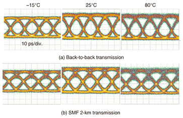
We used the EML with a 150-μm-long EAM to perform a 2-km SMF transmission experiment. We used a 40-Gbit/s, NRZ, 231–1 PRBS while maintaining a constant Vpp of 2.0 V at all operating temperatures. 40-Gbit/s eye diagrams for back-to-back and 2-km-SMF transmissions at –15, 25, and 80°C are shown in Fig. 11. Clear open eyes were obtained in both cases.
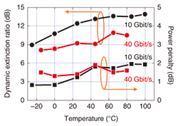
The temperature dependence of the DER and the power penalty for SMF transmission are shown in Fig. 12. A power penalty of less than 2 dB and DER of more than 9 dB were obtained for 10-Gbit/s 80-km SMF transmission. A power penalty of less than 2 dB and DER of more than 8.2 dB were obtained for 40-Gbit/s 2-km SMF transmission.
5. ConclusionWe have demonstrated that two types of 1.55-μm electroabsorption modulator integrated with laser diodes (EMLs) can achieve 10- and 40-Gbit/s wide-temperature-range operation. By designing Δλ to cope with the trade-off relationship between output power and EAM bias voltage (Vb), we achieved output power of 4 mW at 85°C with Δλ of 120 nm at 25°C in an EML with the twin waveguide (TWG) structure. This result shows that the TWG-based EML has the potential to be a candidate for an uncooled light source. LD output power of 14 mW at 85°C was also obtained without the EAM MQW, and we then demonstrated an EML with the butt-joint (BJ) structure to obtain high output power. The Δλ of the BJ structure was designed to obtain a small EAM bias voltage. The Δλ value was designed to be 60 nm at 100°C and Vb of –1.3 V was obtained at 100°C. We then chose the EAM length for 10- and 40-Gbit/s operation. We experimentally confirmed that an EAM length of less than 150 μm enables 40-Gbit/s operation. We fabricated the BJ-based EML using a conventional etching and regrowth process. We achieved a dynamic extinction ratio of over 9 dB from –25 to 100°C for 10-Gbit/s operation and 8.2 dB from –15 to 80°C for 40-Gbit/s operation. Clear eye openings were obtained over a wide temperature range. The power penalty was less than 2 dB for both 10-Gbit/s 80-km and 40-Gbit/s 2-km SMF transmissions over a wide temperature range. These results show that the BJ-based EML is suitable as an uncooled light source for both 10- and 40-Gbit/s transmission. References
|
||||||||||||||||||||||||||||||||||