|
|||||||||||||||
|
|
|||||||||||||||
       |
Special Feature: Front-line Materials Research Vol. 8, No. 8, pp. 7–11, Aug. 2010. https://doi.org/10.53829/ntr201008sf2 Improved Emission Efficiency of 210-nm Deep-ultraviolet Aluminum Nitride Light-emitting DiodeAbstractWe describe technology developed to improve the emission efficiency of our aluminum nitride (AlN) deep-ultraviolet light-emitting diode, which has a wavelength of 210 nm: the shortest wavelength ever observed from any semiconductor. The improvement utilizes the unique characteristic that the emission intensity greatly changes depending on the crystal plane of the emitting surface. 
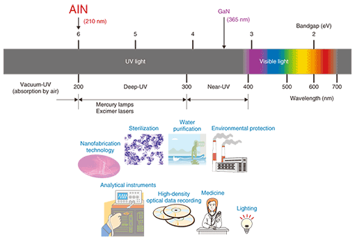
1. IntroductionLight visible to the human eye is in the wavelength range from 400 to 700 nm, as shown in Fig. 1. The color of visible light with the shortest wavelength is violet. Light with wavelengths shorter than 400 nm is called ultraviolet (UV) light. UV light from 300 to 400 nm is called near-UV light, that from 200 to 300 nm is called deep-UV light, and that shorter than 200 nm is called vacuum-UV light. Since vacuum-UV light is absorbed by air, deep-UV light is the shortest-wavelength light that can be used in our living environment.
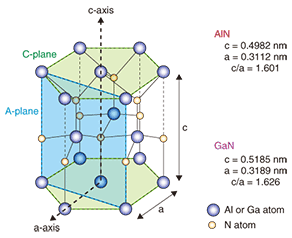
Deep-UV light sources have a wide range of applications. Because shorter-wavelength light has higher photon energy, the photon energy of deep-UV light sources is high enough to kill bacteria and viruses and decompose harmful stable substances, such as dioxin and polychlorinated biphenyls (PCBs), which have caused serious environmental problems all over the world. Therefore, deep-UV light sources are used in water purification, sterilization, and environmental protection equipment. In addition, since the focal point of light decreases with decreasing wavelength, deep-UV light sources have potential for use in high-density optical data recording and nanofabrication technology. Furthermore, they are also expected to be used in medical procedures and analytical instruments. Most deep-UV light sources currently used are gas light sources, such as mercury lamps or excimer lasers. They contain toxic substances, which cause serious environmental problems, and are large in size and low in efficiency and reliability. Moreover, the emission wavelengths are fixed at 254 nm for mercury lamps and 193 nm for ArF excimer lasers. On the other hand, semiconductor light-emitting devices, such as light-emitting diodes (LEDs) and laser diodes (LDs), are harmless to the environment, compact, and highly efficient and reliable. Moreover, the emission wavelength can be tuned by changing the semiconductor’s composition. Therefore, deep-UV semiconductor light sources are of great technological interest as an alternative to toxic large low-efficiency gas sources and will be advantageous for a variety of new applications. 2. UV light-emitting semiconductorsIn a semiconductor, light is emitted when electrons (negative charges) and holes (positive charges) combine. The wavelength of emitted light is determined by the bandgap energy of the semiconductor. Because the emission wavelength is inversely proportional to the bandgap energy, a semiconductor with a higher bandgap energy emits light with a shorter wavelength. For UV light emission at wavelengths below 400 nm, a semiconductor with bandgap energies above 3 eV is necessary. Gallium nitride (GaN), a material used for high-brightness blue LEDs and violet LDs for Blu-ray equipment, has a bandgap energy of 3.4 eV. The emission wavelength is 365 nm, which is in the near-UV region. Near-UV GaN LEDs are now commercially available and are used for white illumination and for the backlighting of liquid crystal displays (LCDs). Like GaN, aluminum nitride (AlN) has a hexagonal wurtzite crystal structure (Fig. 2) and is a direct-bandgap semiconductor with a bandgap energy of 6 eV, the highest among available semiconductors. Therefore, AlN was theoretically predicted to emit light with a wavelength of 210 nm, the shortest value among semiconductors. The emission wavelength of AlGaN, which is a ternary alloy of AlN and GaN, changes from 210 to 365 nm (covering the deep-UV to near-UV regions) as the alloy composition is changed. Therefore, AlN is a key material for UV semiconductor applications.
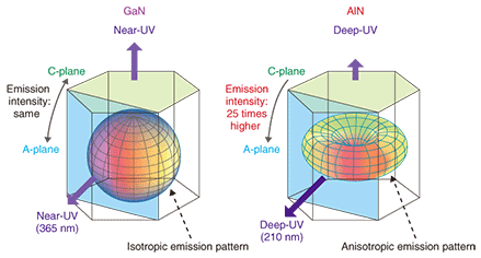
So far, we have developed a method for growing high-quality AlN crystal and technology for its p- and n-type doping [1], [2]. With these technologies, we have successfully demonstrated a deep-UV AlN LED with a wavelength of 210 nm, the shortest wavelength ever observed from any semiconductor. However, the emission efficiency of the deep-UV AlN LED is much lower than that of the near-UV GaN LED. For the deep-UV AlN LED, the key issue for practical use is improved emission efficiency. 3. Emission characteristics of AlNThe reason for the low emission efficiency of the deep-UV AlN LED compared with the near-UV GaN LED is that AlN has directional light emission (strong optical polarization) properties [3]. As shown in Fig. 2, AlN and GaN both have a hexagonal wurtzite crystal structure, which is characterized by its c-lattice constant and a-lattice constant. The crystal has different crystal planes, such as the A-plane and C-plane. Because AlN has higher bond strength and ionicity, it is distorted, so the ratio between the c- and a-lattice constants, c/a, is smaller. Although the difference in the c/a ratio between AlN and GaN is only 1.5%, the difference in their emission properties is large because the physical properties of semiconductors are very sensitive to crystal structural modification. As shown in Fig. 3, like other semiconductors, GaN has an isotropic emission pattern; that is, light is emitted uniformly from all crystal planes. However, for nitride semiconductors, as the c/a ratio decreases, the emission becomes weak parallel to the c-axis direction but strong normal to it (parallel to the a-axis). Therefore, because of its small c/a ratio, AlN has an anisotropic emission pattern where light is barely emitted from the C-plane but is emitted preferentially from the A-plane. The emission intensity from the A-plane is estimated to be 25 times higher than that from the C-plane. This characteristic of AlN is unique among semiconductors.
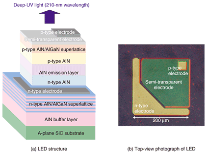
From the viewpoint of crystal growth, the C-plane surface orientation is preferable for growing high-quality AlN and GaN, so C-plane LED structures have usually been fabricated. However, for AlN, because of its stronger A-plane emission, an A-plane LED structure is desirable to enhance light extraction and improve the emission efficiency. 4. Toward high-efficiency deep-UV AlN LEDsWe fabricated the A-plane AlN deep-UV LED structure shown in Fig. 4 [4] by metalorganic vapor phase epitaxy (MOVPE) using an A-plane SiC substrate. Because AlN grows epitaxially on SiC and the difference in lattice constants between AlN and SiC is small, high-quality A-plane AlN layers can be grown. The AlN LED consists of n-type AlN/AlGaN superlattices, an n-type AlN layer, a high-purity AlN light-emitting layer, a p-type AlN layer, and p-type AlN/AlGaN superlattices. In the LED, holes from the p-type AlN and electrons from the n-type AlN are supplied to the light-emitting layer. When the holes and electrons combine, light is emitted. We used the n- and p-type superlattices to reduce the contact resistance of the electrodes.
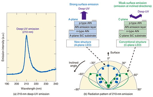
The light emission spectrum of the A-plane AlN LED is shown in Fig. 5(a). When a forward voltage was applied, deep-UV light emission was observed at 210 nm, the same wavelength as for the C-plane AlN LED. The radiation patterns of the A- and C-plane LEDs are shown in Fig. 5(b). Along the surface normal (0°), for the A-plane LED, the emission intensity was maximum. On the other hand, for the C-plane LED, it was weak along the surface normal. These results confirm that the A-plane structure enhances the LED’s surface emission. Thus, for AlN deep-UV LEDs, because the surface orientation strongly influences the emission property, a device design based on AlN’s unique emission properties is important for improved emission efficiency.
5. ConclusionWe fabricated a deep-UV AlN LED with an A-plane surface for high emission efficiency. For semiconductor UV light source applications, we plan to further improve the emission efficiency of the deep-UV AlN LED to the practical level. References
|
||||||||||||||