 |
|||||||||||||||||
|
|
|||||||||||||||||
|
Special Feature: Front-line Materials Research Vol. 8, No. 8, pp. 17–22, Aug. 2010. https://doi.org/10.53829/ntr201008sf4 Graphene Growth on Silicon CarbideAbstractWith the aim of developing a single-crystal graphene substrate, which is indispensable for practical applications of graphene, we are experimentally and theoretically investigating the structural and physical properties of graphene grown on silicon carbide by thermal decomposition.
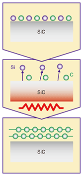
1. IntroductionGraphene is a two-dimensional sheet of carbon atoms in a honeycomb lattice: it corresponds to monolayer (ML) graphite. Although graphene has long been a subject of theoretical investigations, it was not until 2004 that graphene was actually produced by mechanically exfoliating graphene flakes from bulk graphite (exfoliation method) [1]. Since then, graphene has come to be regarded as one of the more promising candidates for an electronics material in the post-Si era owing to its superior electronic transport properties and compatibility with planar lithographic techniques. Graphene has various potential applications. Its huge carrier mobility at room temperature makes it promising as a channel material in field effect transistors. In graphene, carriers can travel long distances without scattering, which is a favorable characteristic for quantum-effect and spintronics devices. Because graphene is highly sensitive to the environment because of its pure two-dimensionality, it is applicable to highly sensitive chemical/biological sensors. Other applications are also expected for graphene sheets comprising from one to a few layers of graphene, which is commonly referred to as few-layer graphene (FLG). FLG exhibits intriguing physical properties, depending on the thickness. For example, owing to its flexibility, transparency, and good conductivity, it could be applicable to flexible transparent electrodes. In the exfoliation method, graphite flakes repeatedly peeled off with adhesive tape to cleave them in two and make them thinner and thinner are deposited on a Si substrate covered with thermal oxide. Exfoliated graphene does not require any special instruments, and the quality is good because it originates from bulk graphite. In general, however, the flakes are small, typically about 10 μm wide, and the yield is low. Though the exfoliation method is suitable for basic physics and device demonstrations, an alternative fabrication method is essential for graphene to become an industry. For large-scale FLG production, methods of growing FLG epitaxially on SiC by thermal decomposition (Fig. 1) are attracting intense interest. When SiC substrates are annealed at high temperatures, Si atoms selectively desorb from the surface and the C atoms left behind naturally form FLG. Because SiC is a wide-band-gap semiconductor, FLG on SiC can serve as a graphene substrate for electronics applications. SiC wafer technology is advancing rapidly in terms of production cost and scale, and our results to date indicate that the thermal decomposition method is indeed suitable for large-scale FLG fabrication.
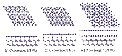
However, two fundamental problems must be solved before the thermal decomposition method can be used industrially. First, the FLG obtained so far has had a thickness distribution. Because the electronic properties of FLG depend on its thickness, we must establish a reproducible way of growing wide, uniform FLG with the desired thickness. Second, we still do not fully understand how the SiC substrate affects FLG’s physical properties. Without a practical assessment of the substrate’s effects, it is difficult to choose the most appropriate applications of FLG. In this article, we describe how we are trying to solve these problems both experimentally and theoretically. 2. Theoretical investigation of graphene growth mechanismTo establish a method of growing large-scale FLG with the desired number of layers, we must clarify the growth mechanism. For this purpose, using a first-principles method, we theoretically calculated stable structures that appear when C atoms are added one by one on the SiC(0001) surface [2]. The stable structures at various C coverages are shown in Fig. 2. We found that, at a C coverage of 8/3 MLs, corresponding to 8 C atoms on three SiC unit cells, C atoms form a graphene-like two-dimensional sheet and are strongly stabilized. Figure 2(a) shows top and side views of the structure. Some C atoms in the two-dimensional sheet form bonds with Si atoms on the SiC substrate. Therefore, the C sheet does not exhibit the electronic band structure characteristic of graphene and is usually called a buffer layer or the 0th layer.
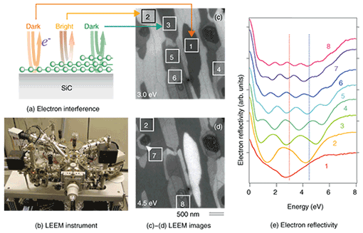
When more C atoms are added, they become highly unstable on the buffer layer and prefer to reside between the buffer layer and SiC substrate, as shown in Fig. 2(b). At a C coverage of 16/3 MLs, a new buffer layer is formed at the interface and the original buffer layer loses bonds with the substrate (Fig. 2(c)). Therefore, the top C sheet possesses an electronic structure similar to that of ideal ML graphene. This top C sheet is ML graphene on SiC. 3. Evaluation of number of graphene layersA method of microscopically evaluating the number of graphene layers is a starting point for optimization of the growth conditions. The number of graphene layers on SiC can be determined from the quantized oscillations of the electron reflectivity [3]. Electrons have wave-like properties, and their kinetic energy determines the wavelength. Therefore, as schematically illustrated in Fig. 3(a), electrons reflected from the graphene surface and graphene/SiC interface can interfere, which causes the electron reflectivity to change periodically as a function of the electron energy and FLG thickness. The number of graphene layers can be determined from the reflectivity oscillations.
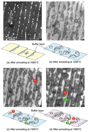
Low-energy electron microscopy (LEEM) is the most suitable technique for this purpose. In the LEEM instrument, electrons with typical energy of a few electronvolts are incident to the surface, and backscattered electrons are used to form magnified images of the surface. A photograph of our LEEM is shown in Fig. 3(b). LEEM images obtained at two different energies are shown in Figs. 3(c) and (d). The LEEM image intensity corresponds to the electron reflectivity. From LEEM images sequentially obtained while the electron beam energy was changed, we obtained the energy dependence of the electron reflectivity from regions 1 to 8, as shown in Fig. 3(e). Periodic oscillations are clearly seen. Thinner FLG provided longer oscillation periods, indicating that graphene sheets 1–8 layers thick were formed on regions 1–8, respectively. 4. Understanding and controlling growth processesLEEM is also suitable for analyzing the graphene growth processes. LEEM images in Fig. 4 indicate structural changes that occurred when the SiC substrate was annealed gradually at high temperatures in an ultrahigh vacuum (UHV) with pressures of less than 10-8 Torr. After annealing at 1060ºC, preferential nucleation of the buffer layer occurred at the atomic steps on the SiC surface, where 1/3 of the ML of Si adatoms was periodically arranged (Fig. 4(a)). After annealing at a higher temperature (Fig. 4(b)), the whole surface was covered with the buffer layer and the surface steps meandered widely. The number of C atoms in ML graphene is nearly equally to the number of C atoms in three SiC bilayers. This means that many atoms moved during the buffer layer formation, which explains the step meandering. At the initial stage of graphene growth, ML graphene preferentially formed near the substrate steps (Fig. 4(c)). When the annealing temperature was further increased, bilayer (BL) graphene appeared before the buffer layer completely disappeared (Fig. 4(d)). This means that uniform ML graphene is difficult to grow in UHV.
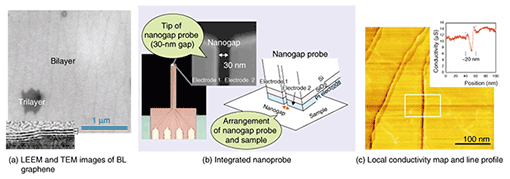
However, we found that further annealing led to relatively uniform BL graphene. Therefore, we focused on optimizing the BL graphene growth conditions. At present, we can grow uniform BL graphene as large as several micrometers square, as shown in Fig. 5(a) [4].
5. Local electrical conductivity measurementsTo understand how the SiC substrate affects the FLG’s properties, we measured the local electrical conductivities of FLG using an integrated nanogap probe (Fig. 5(b)). The nanogap probe contains two Pt electrodes with a gap of 30 nm fabricated at the tip of the cantilever of an atomic force microscopy (AFM) apparatus. As the surface morphology is obtained by AFM, electric currents between the electrodes are simultaneously measured [5], [6]. An electrical conductivity map of BL graphene is shown in Fig. 5(c). Linear contrasts, which correspond to the substrate steps, reveal that the substrate steps modify the electrical conductivity. As shown in the transmission electron microscopy (TEM) image in Fig. 5(a), FLG covered the substrate steps like a carpet. FLG was locally bent near the steps, and this bending could affect the carrier transport. 6. Towards single-crystal graphene substrateOur theoretical investigations have shown that a new buffer layer is repeatedly inserted below the old one. Therefore, FLG always maintains its epitaxial relationship with the SiC substrate. The topmost graphene originates from the initial buffer layer and is continuous everywhere across the substrate step and across the boundary between the regions with different numbers of graphene layers. These results show that the thermal decomposition of SiC is a suitable way of producing a large single-crystal graphene substrate. By optimizing the growth conditions on the basis of the microscopic evaluations of the number of graphene layers, we have succeeded in growing uniform BL graphene a few micrometers in size by UHV annealing. It has been reported that annealing in Ar atmosphere greatly improves the uniformity of ML graphene [7]. This suggests that annealing environment control could be useful for selectively growing FLG with a desired thickness. The local electrical conductivity measurements with the nanogap probe have revealed that the conductivity was modified near the substrate steps. The effects of the SiC substrate on the FLG’s properties should be clarified in more detail. We need to exploit the positive effects and eliminate the negative ones. Furthermore, to expand the possibilities of graphene technology, we need a method of transferring FLG on SiC to other substrates. AcknowledgmentThis work was partly supported by Grants-in-Aid for Scientific Research or KAKENHI (19310085, 21246006) from the Japan Society for the Promotion of Science. References
|
|||||||||||||||||


