|
|||||||||||||||||||||||||||||||
|
|
|||||||||||||||||||||||||||||||
       |
Feature Articles: System LSI Design for Broadband Optical Access Network Systems Vol. 9, No. 3, pp. 6–10, Mar. 2011. https://doi.org/10.53829/ntr201103fa1 System LSI Design Technology for Communications NetworksAbstractThe first set of Feature Articles in this issue describes research and development of system large-scale integration (LSI) technology (also known as system-on-a-chip (SoC) technology) and high-speed front-end electronics for optical access systems being conducted at NTT Microsystem Integration Laboratories. This article provides an overview and the other articles discuss their roles and characteristics well as related design technology and issues. 
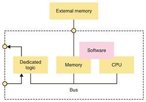
1. IntroductionOpportunities to use a variety of applications on the Internet in daily life are increasing, and Internet access is becoming indispensable. It is desirable for high-quality, convenient, and safe application services to become even more common. This is backed up by the existence of a secure, broadband network services infrastructure utilizing the low losses of optical fiber and the broad bandwidth of light, so networking advances should contribute to a more vibrant, rich, and plentiful society. Optical networks have various components, each playing an important role, including (1) optical devices such as light sources, modulators, transmitters, splitters, and multiplexers; (2) electrical devices that reproduce and process signals and communications protocol controllers; and (3) software that operates them and the communications systems they are part of. At NTT Microsystem Integration Laboratories, one focus of our work is research and development (R&D) of electronics for these communications systems of these types. Among electronic device technologies used in telecommunications systems, ones that we view as particularly important include system large-scale integration (system LSI), which is also known as system-on-a-chip (SoC) technology, which provides sophisticated communications functions, and optical front-end integrated circuits (ICs), which perform high-speed signal processing. SoC technology generally refers to implementations that include a central processing unit (CPU), memory, and large-scale dedicated logic, along with the software to operate it (Fig. 1). SoC technology is used widely, including in general-purpose and household products, but we focus on applications for communications systems using SoC devices (SoCs) that incorporate our experience and knowledge as a communications carrier and contribute to the advancement of communications systems. We are conducting R&D of SoC design technology, including hardware and some of the software, in cooperation with other research laboratories working in the field of communications systems.
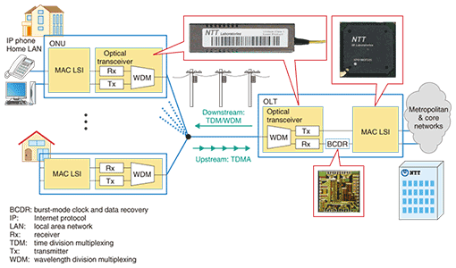
2. SoC design for optical access networksIn Japan, most broadband access services are currently provided by fiber-to-the-home (FTTH) access, and they mostly use the GE-PON (Gigabit Ethernet passive optical network) system [1], [2]. A block diagram of an Ethernet PON system is shown in Fig. 2. A PON allows services to be provided to multiple customers economically by branching a single fiber. It requires the formation of a secure and efficient point-to-multipoint (P2MP) connection between the optical line terminal (OLT) on the network side and the optical network units (ONUs) at the customers’ locations. This is done by sending upstream signals from ONUs to the OLT by using time-division multiple access (TDMA), which is controlled using the multipoint control protocol (MPCP). The main functional components of the OLT and ONU are media access control (MAC) LSIs, which are SoCs, and optical transceivers. The MPCP processing function is implemented in the MAC LSI. Furthermore, the optical transceiver must be able to amplify and regenerate burst frames sent from multiple ONUs when frames have different timings and optical intensities. The electrical components in this optical transceiver are called the optical front-end ICs. At the beginning of system development, functions that could not be included in the SoC were implemented using external components, but as the technology advanced, more of the functions could be integrated into the SoC, reducing the number of parts and overall cost. Standardization of 10G-EPON (10-Gbit/s Ethernet PON), the successor to GE-PON, has recently made progress [2]–[4]. We have responded to this by establishing technology for implementing the standard functions of 10G-EPON in SoCs and optical front-end ICs. We have also conducted feasibility studies on achieving more-sophisticated and higher-performance devices. Below, we discuss the characteristics and technical directions for SoCs and optical front-end ICs in the context of Ethernet PON systems.
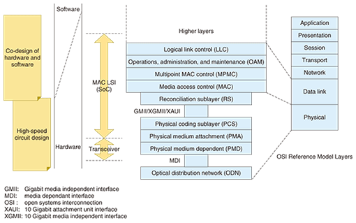
3. Cooperative design of hardware and softwareWhen one is implementing the required functions in an SoC, a major issue is to develop design methods that optimize the partitioning of functionality between functions implemented in hardware with dedicated logic and functions handled by the CPU using software and to generate interfaces between them. For communications operators like NTT, a major concern is whether the systems being developed are flexible enough to accommodate extensions for future services, maintenance, and monitoring functions. Up until now, the general approach to implementing these types of flexible functionality in SoCs has been to use software, but if cooperative design of hardware and software were easier, then circuit configuration and control could be done in more detail, allowing one to pursue both extensibility and flexibility. Moreover, a basic performance requirement for OLTs, ONUs, and, in general, network switches is the capability to process signals at wire speed. To handle the requirements of increased traffic, transmission capacity must be expanded and data must be processed without any frame loss, which places a demand for increased performance on SoCs. To achieve this high performance, hardware techniques for increasing speed play an important role, such as using faster algorithms for logic circuits, parallelization, and pipelining, but we believe that we should also be able to make breakthroughs in power saving for the overall system through better cooperation between hardware and software and by controlling hardware according to actual traffic conditions. 4. MAC LSI functionalityThe P2MP architecture [5] specified in IEEE802.3ah, the standard for Ethernet PON systems, and the way in which the architecture is implemented using MAC LSIs, transceivers, and other components are shown in Fig. 3. Most of the functions required by the system are implemented in the MAC LSI. Most of the functions required by the system are integrated on a single chip, focusing on the various Layer 2 switch (data-link layer) functions from higher-ranking functions such as encryption to physical-layer functions such as encoding and serial/parallel conversion.
5. Research on optical front-end ICsNTT Microsystem Integration Laboratories, together with the NTT Photonics Laboratories, is continually advancing R&D of optical front-end technology. Optical front-end ICs, include amplifiers that reshape in the receiver the weak signals attenuated by transmission through the fiber, digital-data retiming and regeneration circuits, and laser-driver circuits required to produce good quality signals in the transmitter. In the system, these are sections with strict analog requirements, such as sensitivity, feedback or feedforward control, and dynamic range; moreover, they require broadband operation. Furthermore, there is the additional difficulty, mentioned earlier, that data frames arrive at the OLT in burst mode in the PON system. Research issues for these circuits are more physical compared with large-scale SoCs, involving transistor-level circuit design, as well as the physical layout of the circuit and packaging. The selection of semiconductor technology is also an important factor in satisfying performance requirements. We consider (1) compound semiconductors such as InP for heterojunction bipolar transistors (HBTs) and high electron mobility transistors (HEMTs) and GaAs for metal semiconductor field effect transistors (MESFETs), (2) silicon bipolar-junction transistors integrated with complementary metal-oxide semiconductor (CMOS) transistors on a single substrate (Si BiCMOS) including silicon-germanium BiCMOS (SiGe BiCMOS), which integrates SiGe HBTs with conventional CMOS processing, and (3) silicon CMOS (Si CMOS) from cost and performance perspectives and select the optimal technology for a given application. In R&D of optical front-end ICs, there are two key points to consider. First, as with other long-term basic research, it is important to ascertain the feasibility of the technology. When planning and developing innovative services or systems, one must verify in advance whether they are achievable. For example, in order to progress from GE-PON to 10G-EPON, which is a ten-fold increase in transmission capacity, it is necessary to make front-end ICs that are ten times as fast at handling received frames. In particular, the frame header synchronization speed has a great effect on system design with respect to transmission efficiency. Moreover, sensitivity can have an effect on transmission distance or the number of customers that can be accommodated in a single optical distribution network. In this way, the performance levels achievable in the front end have a large effect on overall system specifications, so basic research in this area is done as a precursor to standardization. By conducting R&D in the area that is the physical bottleneck for performance, we will be able to contribute to higher system performance and lead the industry. The second point is that there is synergy in having both SoC technology and front-end technology. Having experience with both makes it easier to study overall optimizations such as controlling the front end from the SoC or optimizing the chip partitioning and interface implementations. We want to use this synergy as one of our strengths in proceeding with R&D. 6. Organization of the Feature ArticlesThis topic has five Feature Articles, including this one which discussed our initiatives related to SoC technology for optical access communications systems and optical front-end IC technology. Next, “Cooperative Hardware/software Design Technology” [6] describes a high-level design technology using virtual hardware effectively for the initial stages of design, including cooperative design. “MAC LSI Design Technology for Optical Access Communications” [7] explains the LSI design process flow and discusses the architecture of an Ethernet PON SoC in detail. “Design Verification Using Field-programmable Gate Arrays for Optical Access Communications SoC” [8] introduces a technology for verifying large-scale SoC functions using field programmable gate arrays before chip prototypes are created. Finally, “10-Gbit/s Burst-mode Receiver Integrated Circuits for Broadband Optical Access Networks” [9] introduces the state of development of optical front-end IC technology for 10G-EPON systems. 7. Future trendsAt NTT Laboratories, we will continue to expand our R&D efforts toward improving the value provided to customers and resolving business issues. To do so, we will continue development of SoC technology in order to further increase system performance, pursue “Green of ICT” much further, and contribute to making systems more flexible by improving customizability and other aspects (ICT: information and communications technology). Until now, the integration level of LSIs has increased according to Moore’s Law* year after year, and this has been the force behind progress in the functionality and performance of semiconductor products. At the beginning of this century, there was some serious discussion about reaching practical limits for reductions in the size of semiconductor processes, but now it appears that some of the fabrication process problems will be solved, and the International Technology Roadmap for Semiconductors (ITRS) [10] has continued to issue roadmaps for still finer technologies. Accordingly, there is hope for continued progress in SoCs and communications systems through R&D driven by leading-edge processes. On the other hand, in addition to active R&D on further miniaturization (more Moore), new functional materials and devices are being developed, in synergy with miniaturization (more than Moore), and research on utilizing more-than-Moore technology for communications systems in the medium-to-long term will also be important.
References
|
||||||||||||||||||||||||||||||