|
|||||||||||||
|
|
|||||||||||||
       |
Feature Articles: R&D of Optical Component Technologies for 100-Gbit/s Digital Coherent Communications Vol. 9, No. 3, pp. 62–67, Mar. 2011. https://doi.org/10.53829/ntr201103fa10 Photodiodes and Transimpedance Amplifiers for 100-Gbit/s Digital Coherent Optical CommunicationsAbstractTo increase transmission capacity and extend transmission distance, 100-Gbit/s digital coherent optical communications systems have been researched. NTT Photonics Laboratories has developed photodiodes that exhibit a good high-frequency response even under high optical input power and transimpedance amplifiers that have both broadband characteristics and a wide input dynamic range. 
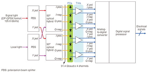
1. IntroductionTo markedly increase transmission capacity and extend transmission distance, 100-Gbit/s digital coherent optical communications systems have recently been researched and developed. The architecture of optical receivers for such systems is shown in Fig. 1. A signal light transmitted through optical fibers (bit rate: 125.6 Gbit/s) and a local light (continuous wave) are input to the optical receiver simultaneously. The local light is necessary in order to decode the signal light, whose signal format is dual polarization quadrature phase shift keying (DP-QPSK). Both the signal light and local light have two optical polarization components (X pol. and Y pol.). Each light is split into beams with different polarizations by polarization beam splitters. Then, the polarization-split lights are fed into 90° optical hybrids. There the signal and local lights are mixed, and two optical-phase-multiplexed components (I and Q, which denote in-phase and quadrature, respectively) in the signal light are separated. The outputs of the 90° optical hybrids are of the differential style, so each hybrid has four outputs (I-pos., I-neg, Q-pos., and Q-neg. (pos.: positive, neg.: negative)). With the polarization beam splitters and the 90° optical hybrids, the signal light, which is both optical polarization multiplexed and optical phase multiplexed, is separated into four independent differential signals. Therefore, the baud rate of each of the four separated differential signals is 31.4 Gbaud, i.e., one-fourth that of the signal light.
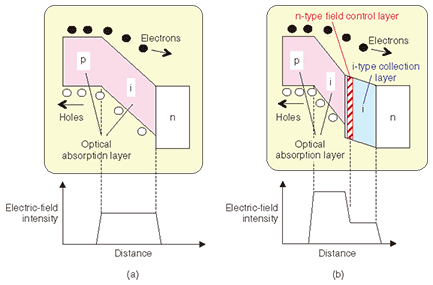
Photodiodes (PDs) convert the high-speed (31.4-Gbaud) optical signals into electrical current ones. To convert four differential optical signals, eight PDs are installed in the optical receiver. Transimpedance amplifiers (TIAs) transform the high-speed electrical current signals into electrical voltage ones, and they linearly amplify the signals to output a constant voltage amplitude that the following analog-to-digital converters can handle. To transform and amplify four differential electrical signals independently, four TIAs are used in the optical receiver. 2. PDs for 100-Gbit/s digital coherent optical communications systemsIn 100-Gbit/s digital coherent optical communication systems, high-power local light is used as one of the inputs for the optical receiver. Therefore, PDs that exhibit a good high-frequency response even under high optical input power are required. To meet this requirement, we have developed a new type of PD called a composite-field maximized-induced-current PD (composite-field MIC-PD) [1]. The energy band diagrams for the conventional MIC-PD and the composite-field MIC-PD are compared in Fig. 2. In the case of the conventional MIC-PD, under high optical input power, the many holes that accumulate in the intrinsic (i-type) optical absorption layer weaken the electrical field and degrade the high-frequency responses of holes and electrons. This effect is known as the space charge effect. In the composite-field MIC-PD, to mitigate the space charge effect, a negative (n-type) field control layer and an i-type wide bandgap collection layer are newly introduced. These layers strengthen the electrical field of the i-type optical absorption layer and lead to improved high-frequency responses of holes and electrons under high optical input power.
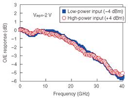
Measured frequency responses for a fabricated composite-field MIC-PD under optical input power of -4 dBm (low-power input) and +4 dBm (high-power input) are shown in Fig. 3. For both inputs, the frequency responses are almost the same. The -3-dB-down frequencies for both inputs are 29 GHz. This result demonstrates that the composite-field MIC-PD relaxes the space charge effect and exhibits good high-frequency responses even under high optical input power.
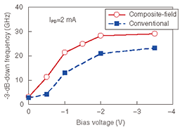
The measured bias voltage dependences of the -3-dB-down frequencies of the composite-field and conventional MIC-PDs are compared in Fig. 4. In the measurement, the photocurrent value was set to 2 mA, which is close to real photocurrent values in 100-Gbit/s systems. While the conventional MIC-PD requires a bias voltage of -3.5 V for a 24-GHz -3-dB-down frequency, the composite-field MIC-PD achieves a 29-GHz -3-dB-down frequency with only a -2-V bias voltage. This shows that the electrical field of the i-type optical absorption layer is sufficiently strengthened with a bias voltage as low as -2 V. The responsivity of the composite-field MIC-PD is around 0.8 A/W, which is also high enough for 100-Gbit/s systems.
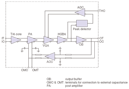
3. TIAs for 100-Gbit/s digital coherent optical communications systemsIn 100-Gbit/s digital coherent optical communications systems, TIAs need to amplify high-speed electrical signals of 31.4 Gbaud. It is empirically known that amplification of a B-baud signal needs bandwidth of 0.7B Hz, where B denotes the baud value. Therefore, TIAs require a broad bandwidth of 31.4 Gbaud × 0.7 = 22 GHz. In addition to the broad bandwidth, TIAs must maintain a constant voltage amplitude in a wide input current range of ~100 μA to ~1 mA In designing a TIA that could satisfy the above requirements, we used InP heterojunction bipolar transistors (HBTs) with a 1-μm-wide emitter. Since these InP HBTs exhibit high-frequency characteristics represented by a high current cut-off frequency (fT) of 170 GHz, they are suitable for designing a TIA with a broad bandwidth of over 22 GHz. The circuit diagram of the TIA that we designed is shown in Fig. 5. Photocurrent from the PDs is fed into the TIA’s input differential terminals IT and IC. Then, the signal is amplified by the following circuit blocks: TIA core, post amplifier, variable gain amplifier (VGA), high-gain broadband amplifier (HGBA), and output buffer. Finally, differential output with a constant voltage amplitude is launched from output terminals OT and OC. To make the output voltage amplitude constant in the whole range of input current, a peak detector and an auto gain control (AGC) circuit are monolithically integrated in the TIA. The peak detector and the AGC circuit compare the real output voltage amplitude of the HGBA with a target amplitude provided through terminal THC, and they control the gain of the VGA so that the output voltage amplitude of the HGBA is equal to the target one. In this way, a function for achieving constant output voltage amplitude is implemented in the TIA. The TIA also contains an automatic offset canceling (AOC) circuit. The AOC circuit excludes DC voltage offset inside the TIA and ensures that high-speed signals are sufficiently amplified. The power supply voltage for the TIA is -5.2 V, and power consumption of one TIA is 660 mW (2.64 W for all four).
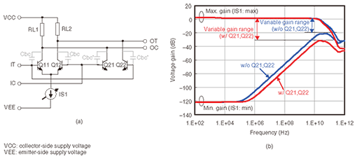
To make the output voltage amplitude constant over the whole range of input current, the VGA gain is controlled by the AGC circuit. Therefore, a variable range of VGA gain is also a key specification for keeping the output voltage amplitude constant, and it should be large enough to correspond to a wide input current range. The circuit configuration of the VGA is shown in Fig. 6(a). The VGA gain is varied by changing current IS1: the gain increases (decreases) with increasing (decreasing) IS1. The simulated frequency-gain characteristics of the VGA for minimum and maximum current IS1 are shown in Fig 6(b). While a large variable range of the gain is achieved at low frequencies, the range is reduced in the high-frequency region because of the increase in minimum gain. This is mainly due to the base-collector capacitances (Cbc) of transistors Q11 and Q12 (Fig. 6(a)), which bypass the high-frequency signal from input to output. To suppress the increase in minimum gain due to Cbc, we added transistors Q21 and Q22 to the VGA. In the circuit configuration in Fig. 6(a), the base-collector capacitances (Cbc’) of Q21 and Q22 cancel Cbc and suppress the increase in minimum gain. As a result, the variable range of the gain is widened by about 10 dB in the high-frequency region.
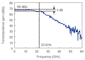
The frequency response of transimpedance gain for a fabricated TIA is shown in Fig. 7. Transimpedance gain at low frequency is 68 dBW (2510 W), and the -3-dB-down frequency is 23 GHz, which exceeds the value required for 100-Gbit/s systems (22 GHz).
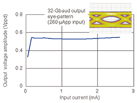
The input current dependence of the differential output voltage amplitude for the fabricated TIA is shown in Fig. 8. Constant output voltage amplitude of 540 mVppd (ppd: peak-to-peak, differential) was confirmed for a wide input current range from 160 μApp to 2.6 mApp. This result shows that the integrated peak detector and AGC circuit successfully controlled the output amplitude to keep it constant. Furthermore, the variable range of the VGA gain was sufficient to keep a constant output amplitude. The inset of Fig. 8 shows a 32-Gbaud output eye-pattern for 260-μApp input. A clear output eye-pattern was observed for the 32-Gbaud input, which is close to the baud rate for practical 100-Gbit/s systems (31.4 Gbaud).
4. ConclusionWe described high-speed photodiodes and transimpedance amplifiers for 100-Gbit/s digital coherent optical communications systems. For the photodiodes, we have newly devised composite-field maximized-induced-current photodiodes and confirmed their good high-frequency responses under high optical input power conditions, which are the characteristics required for 100-Gbit/s systems. We designed and fabricated the transimpedance amplifiers using InP HBTs with a 1-μm-wide emitter and confirmed a broad bandwidth of over 22 GHz and constant output amplitude in a wide input current range. These characteristics are indispensable for 100-Gbit/s systems. In the future, we will research and develop photodiodes that can handle much higher optical input power and transimpedance amplifiers that can keep a constant output amplitude in wider input current ranges. AcknowledgmentThis work was partly supported by the Ministry of Internal Affairs and Communications (MIC) of Japan through the R&D project “High-speed Optical Transport System Technologies”. Reference
|
||||||||||||