|
|||||||||||||||||||||||||||
|
|
|||||||||||||||||||||||||||
       |
Feature Articles: R&D of Optical Component Technologies for 100-Gbit/s Digital Coherent Communications Vol. 9, No. 3, pp. 36–41, Mar. 2011. https://doi.org/10.53829/ntr201103fa6 Optical Device Technologies for Future Network EvolutionAbstractThis article outlines progress in optical device technologies for photonic networks, focusing on integrated optical device technologies for digital coherent optical transmission technologies. With the rapid spread of fiber to the home (FTTH), broadband video services and mobile Internet devices now require a highly functional optical network infrastructure with a large capacity. 
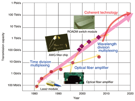
1. IntroductionCommunication traffic has grown owing to the rapid growth of the Internet and broadband services. The technological progress in high-speed and large-capacity optical transmission and the optical devices for optical transmission systems have supported the evolution of information and communications technology. Trends in the transmission capacity of the core network are shown in Fig. 1. From 1980 to the beginning of the 1990s, electrical time domain multiplexing (ETDM) based on on-off keying was the major technology in optical transmission systems. In ETDM systems, high-speed optical and electrical devices as well as optical fiber amplifiers were the keys to achieving high-speed long-haul transmission systems. The total transmission capacity reached 10 Gbit/s. In the 1990s, wavelength division multiplexing (WDM) led to rapid progress in transmission capacity owing to the appearance of optical filters providing optical multiplexing and/or demultiplexing functions. Arrayed-waveguide grating (AWG) technology based on silica-based planar lightwave circuits (PLCs) [1] played an important role in achieving those functions with excellent stability, robustness, and reliability. Since silica-based glass waveguides are formed on the Si substrate in PLC technology, this technology can provide various functions with a very small die area, such as optical multiplexing/demultiplexing, optical switching, and optical attenuation [2]. Here, the optical switching and attenuation is achieved by Mach-Zehnder interferometers with thermo-optic heaters. These PLC technologies are applied to key optical components for not only core networks but also metro-area networks. For example, reconfigurable optical add/drop multiplexers (ROADMs), which feature low latency, flexibility, and upgradability, have been developed using PLC technology. In an ROADM switching module, highly integrated PLC technology containing the AWG and optical switches and hybrid integration technology have been used to achieve a compact and highly functional OADM [3].
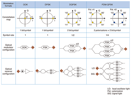
The latest 40-Gbit/s × 40 wavelengths WDM system has been deployed in the core network, and total transmission capacity has reached 1.6 Tbit/s. To keep up with the demand for rapid growth of communication traffic, new technologies supporting 10-Tbit/s optical transmission systems based on 100 Gbit/s per channel (ch) are expected. One attractive candidate technology for 100-Gbit/s-based WDM systems is digital coherent transmission, which combines coherent detection and digital signal processing [4]. In the next section, we review the transmitter/receiver configurations for various optical modulation formats and describe the integrated optical device techniques for digital coherent technology. 2. Optical modulation formats and optical transmitter/receiver configurationsThe configurations of optical modulators and receivers for various optical modulation formats as well as the relationship between symbol and data transmission rates are summarized in Fig. 2. The on and off optical signals were generated in the optical modulator according to the signal information of “1” and “0” in on-off keying (OOK) direct detection modulation. OOK was widely applied to systems with data transmission rates up to 10 Gbit/s because it lets us make a simple optical modulator and receiver configuration. To achieve even greater capacity and long-distance transmission, the important technical issue is how to increase the spectral efficiency while maintaining the tolerance of the optical signal-to-noise ratio. In order to achieve this, optical phase shift keying schemes such as differential phase shift keying (DPSK) and differential quadrature phase shift keying (DQPSK) have been investigated. For example, DQPSK has been applied to the abovementioned 40-Gbit/s/ch WDM systems. In the case of DQPSK, 2-bit signals are modulated and assigned to four optical phases, which results in a two-fold improvement in spectral efficiency compared with OOK. DQPSK is thus able to relax the limitations on both optical bandwidth and transmission distance due to chromatic dispersion. Polarization division multiplexed quadrature phase shift keying (PDM-QPSK) with coherent detection is being investigated for the next-generation 100-Gbit/s/ch systems. PDM-QPSK multiplexes two QPSK signals in the polarization domain. It has the great advantage of mitigating the problems of increasing both the electrical analog amplification bandwidth and the digital signal processing speed because it can reduce the symbol rate to 1/4 of the data transmission rate. As shown in Fig. 2, the configurations of modulators and receivers become complicated when phase shift keying and polarization multiplexing are used. This indicates that highly functional and integrated optical device technology, which provides a small size and low cost, will be important to support future large-capacity optical transmission systems.
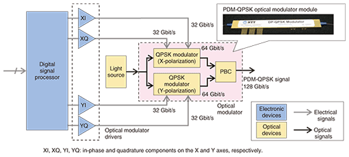
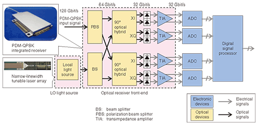
3. Digital coherent technology and optical front-end configurationsDigital coherent technology combines coherent detection and digital signal processing at the receiver side and enables us to use various modulation formats. The transmitter and receiver for a digital coherent system using PDM-QPSK modulation format are shown in Figs. 3 and 4, respectively. Here, the signal data transmission rate is 128 Gbit/s when a forward error correction code that allows a 20% increase in the data rate is used. The transmitter consists of a digital signal processor, a light source, an optical modulator, and modulator drivers, as shown in Fig. 3. Here, the optical modulator comprises two QPSK modulators and a polarization beam combiner (PBC). On the other hand, the receiver consists of a local oscillator (LO) light source, optical receiver front-end, analog/digital convertors (ADCs), and a digital signal processor, as shown in Fig. 4. First, the optical phase information is recovered by mixing the input optical signal with the LO light, and then the signals are converted into electrical signals and linearly amplified in the front-end. After that, the electrical signals are sampled by the ADCs, and the original data signals are then recovered in the digital signal processor by using a phase and amplitude estimation algorithm. Here, the use of the digital signal processing has three important features, which is quite different from the previous technologies: 1) stable phase synchronization between the received optical signal and the local light as well as stable polarization demultiplexing, 2) both adaptive polarization dispersion compensation and chromatic dispersion compensation through the use of sophisticated digital filter technology, and 3) flexible selection of various modulation formats with minimum modification of the hardware.
4. Optical modulator for 100-Gbit/s digital coherent technologyMach-Zehnder interferometers have been widely used as optical amplitude modulators for conventional OOK systems. In this case, the optical phase difference of the interferometer is controlled by external data signals. When the phase difference is 0°, the output optical signal is on, while when the phase difference is 180°, the output optical signal amplitude is off. On the other hand, in QPSK modulation, the phase of the interferometer must be controlled in the range from 0° to 360°, which means that QPSK optical modulators require twice the driving voltage that conventional amplitude modulators do. In addition, a polarization multiplexing function, which combines two QPSK signals in the X and Y polarizations, is indispensable for PDM-QPSK signal generation. Therefore, the PDM-QPSK optical modulator must satisfy two requirements: a low driving voltage and the integration of two QPSK modulators and a PBC. As the material for conventional optical modulators, LiNbO3 has been widely used. It features low chirp and low insertion-loss characteristics. However, there are technical issues in the monolithic integration of a complicated low-loss waveguide and PBC in order to construct a complicated optical modulator for PDM-QPSK. NTT Photonics Laboratories has been investigating PLC-LiNbO3 hybrid technology for those complicated multilevel optical formats [5], [6]. In this technology, various kinds of optical components like optical couplers, PBCs, and splitters are monolithically integrated on the PLC, while LiNbO3 is just used for optical phase modulation. Since a PLC can provide various functions in a small size with high reliability, hybrid technology is advantageous in terms of flexibility for various modulation formats, like PSK and QAM (quadrature amplitude modulation), and scalability to advanced modulation formats [5], [6]. 5. Optical receiver devices for 100-bit/s digital coherent technologyKey optical devices for the digital coherent receiver are the optical receiver front-end and LO light source, as shown in Fig. 4. The receiver front-end consists of optical polarization splitters, 90° optical hybrids, photodiodes, and transimpedance amplifiers (TIAs) [7]. To make small low-cost receivers, technology for integrating these optical and electrical devices is of great importance. The passive optical circuits, for demultiplexing polarization components and mixers for mixing an optical signal with an LO light, are required to have a high polarization extinction ratio at the polarization demultiplexers and a low phase error at the mixers. They have conventionally been implemented using optical fiber or free-space optics technologies. However, those technologies cannot easily provide stable operation with a small size. One promising approach is the application of PLC technology to the monolithic integration of these two functions because a PLC can monolithically integrate 90° hybrids, couplers, and a polarization beam splitter (PBS) on a single Si-substrate [8]. As for the conversion of optical signals to electrical ones in the front-end receiver, the following three performances are required: 1) broadband characteristics able to handle a data rate of 32 Gbit/s, 2) a wide dynamic range for the optical signal input intensity, and 3) linear amplification with low variation in output voltage swing, phase, and skew in each output channel. The TIA is required to provide not only the functions of auto-gain control and output voltage swing adjustment, but also high-gain, broad-bandwidth, low waveform distortion, and low dynamic skew at the same time. To cope with these requirements, several TIAs that use high-speed and high-breakdown voltage device technologies such as SiGe BiCMOS (bipolar complementary metal oxide semiconductor) and InP HBTs (heterojunction bipolar transistors) are being investigated. As for the LO light source, both low phase noise, i.e., narrow spectral line width and high output power, are required because the optical frequency stability affects the phase extraction stability, especially in intradyne coherent detection, and high LO light power is useful for obtaining higher signal input sensitivity. NTT Photonics Laboratories has already demonstrated an L-band tunable laser diode array module that provides a narrow linewidth of less than 580 kHz and high fiber output power of 20 mW [9]. An integrable tunable laser assembly, which integrates light wavelength control with a tunable laser source in one module, will be important for achieving a small transmitter and receiver board. Standardization for the abovementioned optical components for 100-Gbit/s/channel digital coherent transmission, such as optical modulators, integrated optical front-ends, and LO light sources, is currently under way in the Optical Internetworking Forum (OIF) [10]. We will continue to improve our optical device and integration technologies to obtain much higher performance and to contribute to future network evolution by providing new optical device technologies. 6. ConclusionsA 100-Gbit/s/channel system based on digital coherent technology is considered to be a promising candidate for next-generation large-capacity long-distance optical communication systems. The optical components required for such systems, such as a PDM-QPSK optical modulator, integrated receiver, and local light source, are under development. Opto-electrical integration technologies, which enable us to construct small, low-cost, and highly functional optical components, will play an important role in providing cost-effective transmission equipment for future 100-Gbit/s/ch and post-100-Gbit/s/ch optical communications. References
|
||||||||||||||||||||||||||