|
|||||||||||||||||||||||||||||||||||
|
|
|||||||||||||||||||||||||||||||||||
       |
Regular Articles Vol. 9, No. 4, pp. 44–51, Apr. 2011. https://doi.org/10.53829/ntr201104ra2 Flexible-format Optical Modulators with a Hybrid Configuration of Silica Planar Lightwave Circuits and LiNbO3 Phase ModulatorsAbstractWe have devised and fabricated two types of flexible-format optical modulators that let us flexibly change the modulation format: a single-carrier modulator, which supports 4-, 8-, and 16-level modulations, and a multicarrier modulator, which provides a selectable combination of the number of frequency carriers and modulation levels. Both were fabricated using a hybrid integration of silica planar lightwave circuits and LiNbO3 phase modulators and successfully operated at high baud rates corresponding to >100 Gbit/s. These technologies are promising for future spectrally efficient optical networks in which various modulation formats are used flexibly and adaptively. 
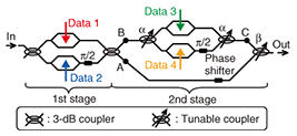
1. IntroductionMultilevel modulation formats, such as N-level phase-shift keying (N-PSK) and N-level quadrature amplitude modulation (N-QAM), are the keys to achieving a large transmission capacity and high spectral efficiency (SE) in wavelength-division multiplexed (WDM) optical transmission systems. A record transmission capacity of 69.1 Tbit/s with SE of 6.4 bit/s/Hz has been achieved using polarization-division-multiplexed (PDM) 16QAM [1]. However, a higher modulation level, which offers higher SE, also leads to lower receiver sensitivity, which means a shorter transmission distance [2]. Because of this trade-off, the choice of modulation level may vary with the system design, so a transmitter that supports multiple modulation formats will be useful. Furthermore, flexible switching of modulation formats in response to optical path switching will be beneficial for maintaining the maximum SE for each channel in future all-optical networks (also called transparent networks) in which signals are switched without optical-to-electrical and electrical-to-optical conversion [3]. To generate multilevel optical signals, multilevel electronics, such as arbitrary waveform generators or digital-to-analog converters, have been used in many transmission experiments [3]–[5]. With such multilevel electronics, we can cover various modulation formats with a simple optical setup. On the other hand, optical multilevel-signal syntheses, in which only binary electronics are used, have also been studied extensively [1], [2], [6]–[10]. Those schemes are promising for high-speed multilevel modulations because binary electronics pose fewer challenges for high-speed operation than multilevel electronics do [6], [7]. However, they have lacked flexibility; different optical configurations have been required for different modulation formats. In this study, we devised two types of flexible-format optical modulator using optical multilevel-signal syntheses. One is a single-carrier flexible-format modulator, which supports 4-, 8-, and 16-level modulation formats [11]. The other is a multicarrier flexible-format modulator, which provides frequency-division-multiplexed (FDM) multilevel modulation with a selectable combination of the number of frequency carriers and modulation levels [12]. Both modulators let us change the SE at the cost of a reduced transmission distance without changing the baud rate. The main difference is that the single-carrier type changes the bit rate and keeps the spectral bandwidth, while the multicarrier type changes the spectral bandwidth and keeps the bit rate. We fabricated them using a hybrid integration of silica planar lightwave circuits (PLCs) and LiNbO3 (LN) phase modulators, which is promising for fabricating advanced multilevel modulators with both a large electro-optic bandwidth and complicated optical configurations [10]–[13]. The modulators successfully operated at high baud rates corresponding to bit rates of >100 Gbit/s. 2. Single-carrier flexible-format modulator2.1. Design and fabricationThe single-carrier modulator was designed to support quadrature-PSK (QPSK), 8PSK, 8QAM, and 16QAM. These 2N-level signals (N=2, 3, 3, and 4, respectively) can be generated through optical signal syntheses using N binary-driven Mach-Zehnder modulators (MZMs) [6]. We designed the modulator so that it has four MZMs and tunable circuits with which we can select the number of MZMs contributing to the modulation. The optical-circuit configuration of the modulator is shown in Fig. 1. It has a two-stage lattice configuration. In the first stage, each arm has an MZM. In the second stage, the upper arm has two MZMs connected in parallel plus a pair of tunable couplers while the lower arm does not have any functional components. The couplers at the input of the first stage and between the first and second stages are static 3-dB couplers, while the one at the output of the second stage is another tunable coupler. The four MZMs (denoted MZMs 1–4) are driven in push-pull conditions with different binary data signals, Data 1–4, respectively. All data signals have an amplitude of 2Vπ, so the MZMs operate as binary-PSK (BPSK) modulators. MZMs 2 and 4 are followed by π/2 phase shifters. The power coupling ratios of the tunable couplers, α:1-α and β:1-β (upper to lower arms), as denoted in the figure, are varied for different modulation formats. The relative optical phase between the upper and lower arms of the second stage, φ, is also varied.
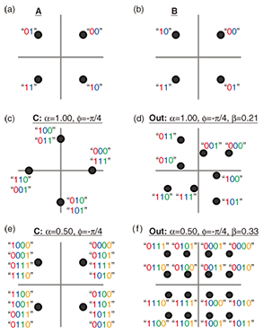
The operating principle is as follows. The signal constellations at points A, B, and C and at the final output port are shown in Fig. 2. Here, the data values 1 and 0 are allocated to optical phases 0 and π, respectively, in each BPSK signal generated with an MZM. A binary data string at each signal point (e.g., 1100) represents the values of Data 1–4 from left to right. As shown in Figs. 2(a) and (b), the first stage sends two QPSK signals to the two arms of the second stage. Those two signals have the same amplitudes but different (mirror-symmetric) data mappings. By setting β=0, we can obtain the QPSK signal shown in Fig. 2(a) as the modulator’s final output. An 8QAM signal is generated when α=1, φ=-π/4, and β=1/(3+
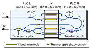
We fabricated the modulator with the configuration shown in Fig. 3. We used two PLCs (PLC-L and -R) and an X-cut LN chip and implemented the modulator circuit with a compact loop-back configuration. The LN chip has an array of eight straight phase modulators, four signal electrodes (coplanar waveguides), and a passive straight waveguide. The PLCs contain all other circuit components: Y-branches for MZMs, 3-dB wavelength-insensitive couplers (WINCs), tunable couplers, and U-turn waveguides. Each tunable coupler consists of Mach-Zehnder circuits with a thermo-optic phase shifter in each arm. We bonded the chips to each other with ultraviolet-curable (UV-curable) adhesive and then mounted them on an SUS package with radio-frequency connectors. The PLC-L, LN, and PLC-R chips are 29.0 mm × 6.5 mm, 64.0 mm × 6.0 mm, and 17.0 mm × 6.5 mm, respectively, giving a total chip length of 110 mm.
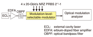
2.2. CharacteristicsAt a wavelength of 1550 nm, the insertion loss of the modulator with β=0 is 7.3 dB and that with β=1 and α=0.5 is 7.5 dB. The difference of 0.2 dB corresponds to the excess loss in MZMs 3 and 4 and in the two tunable couplers. The 3-dB bandwidths of the electro-optic frequency responses are around 25 GHz for all MZMs. We tested the modulator in the single-polarization back-to-back setup shown in Fig. 4. The light source was an external-cavity laser with a wavelength of 1551 nm and linewidth of ~30 kHz. The modulator was driven with four 20-Gbit/s non-return-to-zero (NRZ) 211-1 pseudo-random bit sequences (PRBSs) with different delays. We switched the modulation formats by using the tunable couplers as described above, while making no change in the driving signals. The output optical signal was received with an optical modulation analyzer (Agilent Technologies, N4391A), combined with a 50-gigasample-per-second (GS/s) storage oscilloscope (Tektronix Inc., DPO72004B), and analyzed offline.
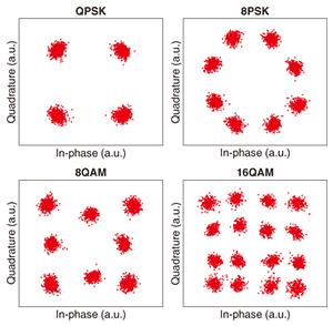
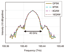
As shown in Fig. 5, clear constellations were obtained for the 20-Gbaud QPSK, 8PSK, 8QAM, and 16QAM signals, which correspond to 80, 120, 120, and 160 Gbit/s, respectively, if we use PDM. The bit-error rates (BERs) for QPSK, 8PSK, and 16QAM were <10-6 (no errors in 2×10⁶ symbols), 1.9×10⁻⁵, and 3.1×10⁻⁴, respectively. BER measurement for 8QAM is not currently supported by the analyzer software, but the BER was estimated to be well below 10-4 from the measured error-vector magnitude of 9.8%. Optical signal spectra with these four formats are shown in Fig. 6. They almost completely overlap and their main-lobe bandwidths are 40 GHz.
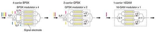
3. Multicarrier flexible-format modulator3.1. Design and fabricationThe multicarrier flexible-format modulator was designed to support four-carrier BPSK, two-carrier QPSK, and one-carrier 16-QAM. With a fixed baud rate, all these formats give the same bit rate. By increasing the modulation level and decreasing the number of carriers, we can increase the SE at the cost of reduced receiver sensitivity (transmission distance) [3]. If we were to design separate modulators for the three formats, we would use some straightforward optical-circuit configurations such as those shown in Fig. 7. The four-carrier BPSK modulator consists of three interleave filters (ILFs) for demultiplexing carriers, four MZMs as four BPSK modulators, and three 2×1 couplers. The two-carrier QPSK modulator consists of one ILF, two pairs of MZMs as two QPSK modulators, and one 2×1 coupler. The one-carrier 16-QAM consists of a parallel-quad MZM as a 16-QAM modulator. These modulators have almost the same configuration except for certain passive components, such as the ILFs and couplers.
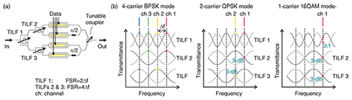
To provide these three configurations in a common design, we devised a modulator with a novel configuration consisting of three tunable ILFs (TILFs), four MZMs, two 2×1 couplers, and one tunable coupler as shown in Fig. 8(a). To use the modulator as a four-carrier BPSK modulator (four-carrier BPSK mode), TILFs 1–3 are operated normally as carrier-demultiplexers, as shown in Fig. 8(b), and then the tunable coupler is set with a 3-dB coupling ratio. To use the modulator as a two-carrier QPSK modulator (two-carrier QPSK mode), TILFs 2 and 3 are changed so that they operate as 3-dB couplers at the carrier frequency for carrier channels 1 and 2, respectively, to tune the phase condition of the TILFs. For use as a 1-carrier 16-QAM modulator (1-carrier 16-QAM mode), TILFs 1–3 are changed so that they operate as couplers with coupling ratios of two-to-one, 3 dB, and 3 dB, respectively, at the carrier frequency, and then the tunable coupler is set with a two-to-one coupling ratio. Thus, the devised modulator lets us select the modulation format flexibly from among three formats: four-carrier BPSK, two-carrier QPSK, and one-carrier 16-QAM.
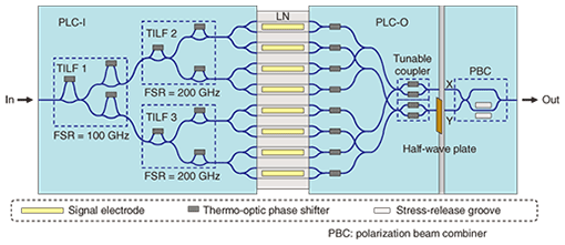
The configuration of the fabricated modulator, which generates an optical signal with a total rate of 200 Gbit/s by using eight 25-Gbaud electrical signals in dual polarization operation, is shown in Fig. 9. We used two PLCs (PLC-I and -O) and an X-cut LN chip. The LN chip has an array of sixteen straight phase modulators with eight signal electrodes (coplanar waveguides). PLC-I consists of three TILFs and 1×2 couplers. Each TILF is composed of three Mach-Zehnder interferometers (MZIs) with thermo-optic phase shifters. One MZI is the main TILF, which has two output ports. The others, which have only one output port each, are added to obtain high isolation for demultiplexing. The free spectral range (FSR) of TILF 1 is 100 GHz. TILFs 2 and 3 each have an FSR of 200 GHz. PLC-O consists of 2×1 couplers, thermo-optic phase shifters for IQ (in-phase and quadrature) phase tuning, tunable couplers, a half-wave plate as a polarization rotator, and a polarization beam combiner. The polarization beam combiner consists of an MZI with stress-release grooves to control waveguide birefringence [14]. We arranged the MZMs in an alternating layout to share the TILFs for X- and Y-polarizations. We bonded the chips to each other with UV-curable adhesive and then mounted them on an SUS package with radio-frequency connectors. The PLC-I, LN, and PLC-O chips are 33 mm × 13.5 mm, 64 mm × 6.0 mm, and 35 mm × 4.4 mm, respectively, giving a total chip length of 132 mm.
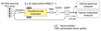
3.2. CharacteristicsThe insertion loss of the modulator was 8.8 dB at a wavelength of 1550 nm when all the thermo-optic phase shifters were tuned so that the transmittance was maximum. The 3-dB bandwidths of the electro-optic frequency response were around 25 GHz for all the MZMs. We tested the modulator in the back-to-back self-homodyne setup shown in Fig. 10. Four tunable laser diodes (TLDs) with 50-GHz spacing were used as a multicarrier light source. The modulator was driven with eight 25-Gbit/s NRZ 211-1 PRBSs with different delays for 200-Gbit/s operation. We changed the modulation modes by using the TILFs and tunable couplers as described above, while making no change to the driving signals. The number of TLDs constituting the multicarrier source and the TLD wavelengths were changed with the modulation mode. The output optical signal was received with an optical spectrum analyzer and an optical modulation analyzer, combined with a 50-GS/s storage oscilloscope, and analyzed offline. To enable self-homodyne detection to be used for constellation measurement, the light from the TLD corresponding to the measured carrier channel was changed to that from the local-oscillator in the optical modulation analyzer.
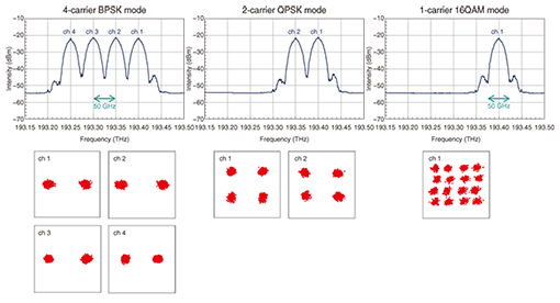
Measured optical output spectra and constellations of X-polarization signals transmitted via a polarization beam splitter are shown in Fig. 11. Those for the Y-polarization signals were almost the same. Clear spectra and constellations were obtained in each modulation mode. This means that we were able to select the operating format as four-carrier BPSK, two-carrier QPSK, or one-carrier 16-QAM. The signals with all these formats have the same bit rate of 200 Gbit/s with a symbol rate of 25 Gbaud. Although we used FDM with a frequency spacing twice the baud rate in this first demonstration, we can also readily cover orthogonal frequency division multiplexing (OFDM), in which the frequency spacing equals the baud rate, by changing the FSR of the TILFs.
4. ConclusionWe devised and demonstrated single-carrier and multicarrier flexible-format modulators fabricated with a hybrid configuration of PLCs and LN phase modulators. These modulators let us flexibly select the modulation format simply by using tunable optical circuits while driving the data electrodes with only 2Vπ binary signals. Thanks to the hybrid configuration, the modulators show small optical insertion losses of 7.5 and 8.8 dB, respectively, despite their complicated optical configuration. Flexible-format operations with high baud rates corresponding to bit rates of >100 Gbit/s were successfully demonstrated. These technologies are promising for future optical networks in which various modulation formats will be used flexibly to exploit spectral resources efficiently. References
|
||||||||||||||||||||||||||||||||||