|
|||||||||||||||||||||||||||||||||||||||||||||||||||||||||||||||||||||||
|
|
|||||||||||||||||||||||||||||||||||||||||||||||||||||||||||||||||||||||
       |
Regular Articles Vol. 9, No. 5, pp. 36–45, May 2011. https://doi.org/10.53829/ntr201105ra1 Monolithic Integration of Silicon Photonics Devices for Telecommunications ApplicationsAbstractThis article introduces our recent progress in silicon photonics device integration for telecommunications applications. We have developed new processes for selective epitaxial growth of Ge on a Si waveguide core and for low-temperature deposition of silica waveguide film. Using these processes, we have managed to monolithically integrate Si variable optical attenuators (VOAs) with a Ge photodetector and Si VOAs with a silica arrayed waveguide grating. These integrated devices exhibit sufficient performance for application to future telecommunications systems that combine wavelength-division multiplexing and burst-mode packets. 
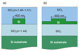
1. IntroductionThe rapid and huge increase in telecommunications traffic requires highly integrated photonic devices, which make possible high-functionality, low-power, and low-cost telecommunications modules. Recently, photonic integration has been intensively pursued by applying silicon (Si) photonics technology because photonic devices made of Si have many advantages, such as ultrasmall size, low cost, and convergence with electronic devices. A more detailed review of recent R&D trends in Si photonics is given in [1]. Various passive and dynamic devices, such as wavelength filters and modulators, have already been developed using an ultracompact Si wire waveguide, which is a promising platform for photonic integration [2]–[7]. Moreover, some active devices, such as photodetectors (PDs) and light sources have recently been developed on a Si wafer by using heteroepitaxy technology for germanium (Ge) and wafer bonding technologies for III-V materials [8]–[11]. We can now make various individual photonic devices on the Si platform, and some devices, such as filters, modulators, and PDs are already at a level suitable for practical application. As device integration on a chip is the most important advantage of Si photonics, research on Si photonics is now shifting to the integration of devices having various photonic functions. In this article, we describe two optical device integrations for telecommunications applications. One is the integration of a Si variable optical attenuator (VOA) and a Ge PD and the other is the integration of Si VOAs and a silica-based arrayed waveguide grating (AWG) filter. The VOA-PD integrated device allows high-speed optical level control, which is very important for suppressing fast gain transients and equalizing gain variations. The VOA-AWG integrated device provides wavelength demultiplexing and high-speed power-level adjustment in individual channels. These integrated devices should be applicable to future telecommunication systems that combine wavelength-division multiplexing (WDM) and burst packets. 2. Fundamental characteristics of Si wire waveguideCross-sectional structures of Si wire waveguides are shown in Fig. 1. We have developed two types of Si wire waveguides: the single-mode channel type and the rib type. Both types consist of a Si core and silica-based cladding and are fabricated on a silicon-on-insulator (SOI) wafer with a buried SiO2 layer of 3 μm. The thickness and width of our waveguide core are roughly in the ranges of 200–300 nm and 300–600 nm. The rib-type waveguide is mainly used for dynamic devices such as attenuators and modulators based on carrier injection because the p+ and n+ regions can be formed in the slab areas. The channel-type waveguide is used for passive devices such as wavelength filters. The Si wire waveguide has a very high refractive index contrast. This is advantageous for high-density integration because it allows the core to be less than a micrometer wide and the bending radius to be just a few micrometers.
Transmission characteristics of our Si wire waveguide for 1550-nm infrared light are shown in Fig. 2. To reduce the coupling loss to an external fiber, our waveguides have spot size converters (SSCs) at both ends. Each SSC consists of a Si inverse taper and a low-index waveguide with a large core covering the taper [2], [13]. For the measurement, high-numerical-aperture fibers with a 4.3-μm field diameter were butt-coupled to the SSC’s low-index waveguide. The slope of the line in the figure shows propagation loss, which is typically around 1 dB/cm. This is for transverse electric (TE) polarization, but the propagation loss for transverse magnetic (TM) polarization is rather lower. The loss of the Si wire waveguide depends largely on the sidewall roughness of the Si core. Improvements in the fabrication technique have greatly reduced the loss due to sidewall roughness [12]. In Fig. 2, the transmittance corresponding to waveguide length = 0 shows the coupling loss for two converters; one coupling loss is about 0.5 dB. The superior performance in propagation and coupling will satisfy the severe telecommunication standards for insertion loss.
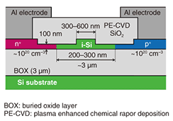
3. Monolithic integration of Si VOA and Ge PD3.1 Device structure and characteristicsSince Si has semiconductor characteristics, we can easily implement various electronic device structures, such as PN (positive, negative), PIN (positive, intrinsic, negative), and MOS (metal oxide semiconductor) structures [5], [14]–[16], which give optical modulation ability through the carrier plasma effect. We have developed a Si VOA with PIN-type carrier injection structures in the rib-type Si wire waveguides [16]. The cross-sectional structure of the Si VOA is shown in Fig. 3. The rib-type Si waveguide has a 600 nm × 200 nm core and 100-nm-thick slab. The p+ and n+ regions are 1 mm long and defined in the slab section, and they are about 3 μm apart. The VOA based on Si wire waveguides has the following advantages. The smaller the core is, the faster the device works. Moreover, because of its ultrasmall core, the carrier density, which determines the optical absorption, can be easily increased, so the size and injection current, or power consumption of the device, can be reduced. We have already demonstrated these advantages in our fabricated devices. For example in a 1-mm-long VOA, the 3-dB frequency bandwidth is over 100 MHz, which is about ten times higher than that in conventional devices. Operation with 30-dB attenuation in a 1-cm-long device requires about 55 mW, which is about half the power consumption of conventional rib-type devices [17]. As this fast VOA is based on a simple structure, a polarization-independent VOA can be achieved just by optimizing the Si core size [18].
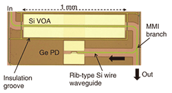
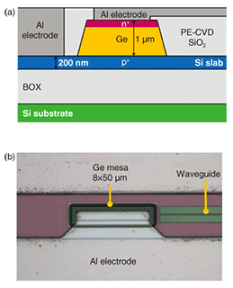
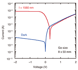
PDs made from Ge are preferred in Si photonics because Ge has process compatibility with Si as well as a large absorption coefficient at telecommunication wavelengths. Recently, we have successfully integrated PIN-type Si VOAs and Ge PDs [19], [20]. A schematic of a fabricated VOA-PD integrated device is shown in Fig. 4. The device consists of a Si VOA, a 3-dB multimode interferometer (MMI) branch, and Ge PD. The MMI branch was placed between the Si VOA and Ge PD to route light to the outside for device evaluation. The vertical cross-section of the Ge-PD and its top view are shown in Fig. 5. The Ge PD is based on a vertical PIN photodiode. A Ge mesa was grown on a Si waveguide by selective epitaxial growth in an ultrahigh vacuum chemical vapor deposition (UHV-CVD) chamber [21]. A SiO2 film that acts as the overcladding of the Si waveguides was used as a mask for the Ge selective growth. The thickness and size of the Ge mesa were fixed to 1 μm and 8 × 50 μm2, respectively. To prevent electrical crosstalk between each VOA and PD through the Si layer, an insulation groove is made around the VOA. For device characterization, we injected 1560-nm-wavelength light with a TE-like mode through a lensed fiber into the waveguide with a 3-μm-expanded core at both edges. The infrared light input into the VOA was split by the MMI branch at the VOA’s exit waveguide. One of the outputs was fed to a Ge PD on the chip and the other to an external fiber. The propagated optical power was attenuated by carrier absorption when carriers were injected into the waveguide.
The current-voltage (I-V) curves of a Ge PD in dark and illuminated condition are shown in Fig. 6. Dark current (Idark) was as low as 60 nA at 1 V of reverse bias, corresponding to a dark current density of 15 mA/cm2. Such a low Idark can guarantee sensitivity as high as -41 dBm in the detectable minimum light power. When light was injected into the waveguide, a photocurrent was generated as shown in Fig. 6. The estimated responsivity was around 0.8 A/W at reverse bias of 1 V. The 3-dB frequency bandwidth of the Ge PD was a few gigahertz, which is limited simply by the RC time constant.
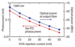
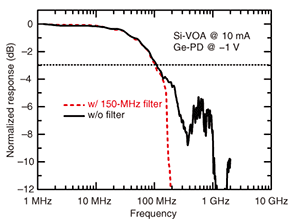
The photocurrent detected at the Ge PD on-chip and optical powers monitored at the output fiber under the condition of VOA current injection are shown in Fig. 7. Since attenuation is linearly proportional to carrier density in the intrinsic region of a VOA, the attenuated optical power in decibels decreased linearly with respect to the injection current. The change in photocurrent corresponds well to the optical power. This indicates that the PD precisely detected the light intensity attenuated by the VOA. Leakage current between the two devices was not observed in synchronous operation because of the insulation groove made around the VOA. We confirmed that both devices fabricated in monolithic integration worked synchronously with good performance. The frequency responses of the VOA-PD integrated device are shown in Fig. 8. Regardless of the reverse bias at the PD, the 3-dB cut-off frequency in VOA-PD synchronous operation was about 130 MHz. The 3-dB cut-off frequency of the VOA was around 130 MHz, while that of the PD was in the gigahertz range. The frequency response of an integrated VOA-PD device is limited solely by the VOA.
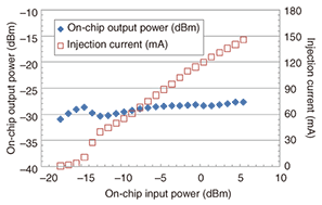
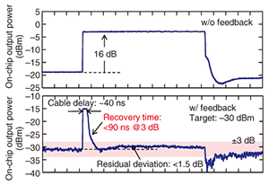
3.2 Application to optical power equalizationOne of the most promising applications of the VOA-PD integration is fast optical power equalization for burst optical packets. For example, power equalization of bursty upstream optical packets can enhance the dynamic range of receivers [22]. Since the response time should be a few hundred nanoseconds in a 10-Gbit/s passive optical network (PON) system [23], the 130-MHz frequency response of our integrated VOA-PD is sufficient for this fast power equalization. To confirm the feasibility of the fast optical power equalization, we attempted optical intensity equalization using our VOA-PD device and an off-chip electrical feedback circuit [24]. The feedback circuit was a simple linear system. The photocurrent of the Ge PD was converted into a voltage signal through a transimpedance amplifier (TIA). The output voltage of the TIA was amplified by a differential amplifier with respect to a voltage reference, which represented the target power level for optical output. Then, the signal was guided to the VOA driver, where injection current proportional to the control voltage signal was generated. The feedback circuit covered a frequency bandwidth from DC to 180 MHz. The output optical power versus input power in DC feedback operation is shown in Fig. 9. The output power stabilized within a deviation of 2.7 dB even when the input power varied by 22 dB. For 10-dB input variation, output stabilization within a deviation of 0.8 dB was accomplished. The VOA injection current exhibited a monotonic increase with no irregular behavior. This indicates that the feedback circuit worked very stably even for a large dynamic range of more than 25 dB in optical input. The temporal response of the output for a step-wise increase in the input level is shown in Fig. 10. When the input optical power suddenly increased by 16 dB, the output power was quickly recovered and stabilized within a 1.5-dB residual error. The 3-dB recovery time was about 90 ns, which will satisfy the timing criterion for burst optical packets in a 10G-EPON (10-Gbit/s Ethernet PON) system. The recovery time includes a 40-ns insensitive cable delay, which could be eliminated by mounting an application-specific integrated circuit on the VOA-PD chip.
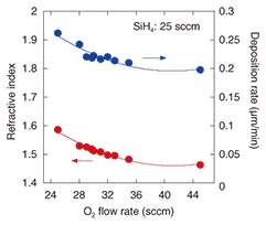
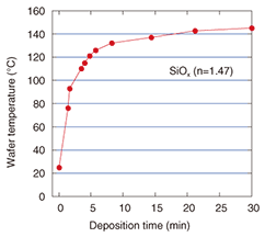
4. Monolithic integration of silicon-based dynamic and silica-based passive devices4.1 Low-temperature deposition of silica waveguide filmsSilica-based waveguides are very attractive for constructing high-performance passive photonic devices, such as AWG wavelength filters and interferometers for receiver circuits because low propagation loss and small polarization dependence are expected [25]. On the other hand, Si wire waveguide devices have other excellent features, such as very fast operation, low power consumption, and high integration density. Therefore, integrating a Si waveguide device with a silica waveguide device should lead to high-performance practical devices for telecommunications applications. A serious obstacle to the integration of Si and silica is the thermal degradation of the Si devices during the fabrication of a silica waveguide. Silica waveguide fabrication generally involves a high-temperature process at over 1000oC in silica film deposition [26]. Such a temperature oxidizes the Si waveguide core and destroys the PIN structures for Si modulation devices and Ge PDs. For Si and silica device integration, we need a low-temperature silica film deposition method. We have recently developed one based on electron-cyclotron-resonance plasma enhanced chemical vapor deposition (ECR-PECVD). The ECR plasma easily dissociates gas molecules and provides moderate energy to the substrate. This enables fast deposition of high-quality silica and silicon-rich silica (SiOx) films at low temperatures. The refractive index and deposition rate of silica film by ECR-PECVD with a mixture gas of SiH4 and O2 are shown in Fig. 11. In this experiment, the SiH4 flow rate was maintained at 25 sccm and the O2 flow rate was changed. The results indicate that the silica film refractive index can be controlled over a wide range from 1.47 to 1.60 by forming SiOx (Si-rich oxide), which is achieved simply by adjusting the flow rate of oxygen. The deposition rate is about 150 nm/min, which is high enough for waveguide films that need a thickness of a few micrometers. The wafer temperatures during the ECR-PECVD of silica film, which were measured with thermosensitive tape put on the wafer surface are shown in Fig. 12. Although the wafer was not cooled purposely, the wafer temperature was below 150oC throughout the deposition time of 30 min, which corresponds approximately to a 2-μm-thick deposition.
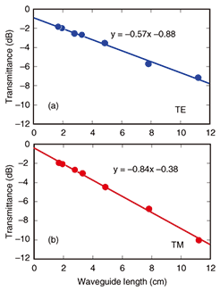
To evaluate the optical loss of SiOx made by ECR-PECVD, we made SiOx waveguides with a refractive index contrast of about 3%. The core was made of SiOx, whose refractive index is 1.515, and the size was 3 μm square. The overcladding was SiO2, whose refractive index is 1.47. These films were formed on 3-μm-thick thermal SiO2 on a Si wafer because the SiOx waveguides were integrated with Si waveguides on an SOI wafer with 3-μm buried SiO2. The transmittance of SiOx waveguides for TE and TM modes as a function of waveguide length is shown in Fig. 13. From the slope of the fitted line, we obtained propagation losses of 0.57 dB/cm for the TE mode and 0.82 dB/cm for the TM mode. These values are low enough for making a practical device on a small chip. The larger loss of the TM mode is probably due to leakage of the propagated light to the Si wafer. The minimum bending radius of this waveguide is 0.5 mm, which will significantly reduce the device size.
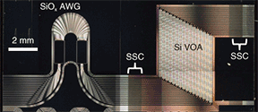
4.2 Si VOA and SiOx AWG integrationUsing the low-temperature silica deposition technique, we have fabricated an integrated variable attenuator multiplexer/demultiplexer (VMUX/DEMUX) [27], which is an important component for photonic networks, such as a reconfigurable optical add/drop multiplexing (ROADM) system. The VMUX/DEMUX consists of VOAs for optical power-level control, PDs for power-level monitoring, and an AWG for WDM. An optical microscope image of the fabricated device is shown in Fig. 14. The device was made by the monolithic integration of Si-VOA and SiOx AWG on an SOI wafer with a 3-μm-thick buried oxide layer. The AWG was made with SiOx waveguides of D 3% and enables wavelength demultiplexing of the C-band signal in 16 channels with 200-GHz spacing. The Si VOA is 5 mm long and its structure is based on the PIN carrier injection described in section 3.1. The AWG provides wavelength demultiplexing and the VOAs quickly adjust the power level in each channel.
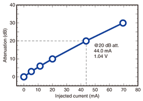
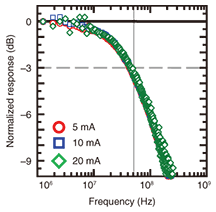
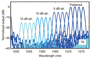
The silica and Si waveguide have very different dimensions. The SiOx waveguide, which composes the AWG, has a cross section of 3 × 3 μm2. The Si wire waveguides, which compose the VOA, have a 0.2-μm core height, 0.6-μm core width, and 0.1-μm slab thickness. The large difference in core size causes a large coupling loss between two waveguides. This is another problem in the integration of Si and silica waveguides. We used an SSC to compensate for the mode-size mismatch and connect them with low loss. Each output port of the AWG is connected to a Si pin-type VOA through SSCs. An SSC consists of a Si inverse taper and a low-index waveguide with a large core covering the taper [20]. The taper, which gradually becomes thinner toward the end, is 300 μm long and the tip is 80 nm wide. A low-index waveguide over the Si taper is made from a SiOx waveguide, which has an about-3-μm-square core and index contrast of about 3%. In this device, the same SiOx layer is used for the cores of the AWG’s waveguides, the cores of the low-index waveguide over the Si taper of the SSCs, and the overcladding of the Si wire waveguide. The sharing of SiOx layers for different purposes simplifies the fabrication process. First, we examined the performance of the integrated Si VOAs. The relationship between attenuation and injected current is shown in Fig. 15. In these experiments, the DC source was connected to the electrode pads of the VOAs. The Si VOA exhibited linear operation as a function of injected current and had a dynamic range up to 30-dB attenuation with an injected current of 70 mA. The power consumption for 20-dB attenuation was 45.8 mW (44.0 mA, 1.04 V). These characteristics are almost the same as those of the stand-alone VOA, indicating that the ECR-PECVD process did not affect the PIN structure in the waveguide. The measured frequency response is shown in Fig. 16. The VOA had a 3-dB bandwidth of about 50 MHz. This frequency bandwidth is sufficient for level equalization for burst optical packets in a 10-Gbit/s PON system. Next, as a demonstration of multichannel power equalization using the VMUX/DEMUX, we operated the VOAs individually and measured the transmission spectrum of each channel. The measured spectra are shown in Fig. 17. We separated the channels into groups of four and drove the VOAs so that all the channels in a group had the same intensity. We can see that the VOAs independently set the optical level in a group. We verified that all of the integrated VOAs operated, and we drove them so that the transmission level was equivalent every four channels. This device exhibits wavelength demultiplexing owing to the AWG and high-speed power-level adjustment in individual channels owing to the Si-VOA, which has a 3-dB bandwidth of about 50 MHz. The fast level control on each wavelength channel will be useful in future burst-mode WDM telecommunications networks.
5. ConclusionWe demonstrated the monolithic integration of a Si-wire-based VOA, Ge PD, and SiOx-based AWG. To integrate photonic devices made of different materials, we developed new processes, including selective epitaxial growth of Ge on a Si core, and a low-temperature method of silica film deposition. The Si VOA and Ge PD integrated device showed good synchronous operation with a bandwidth of around 100 MHz, which is limited by the VOA. We demonstrated that this device can work as a fast intensity equalizer for burst-mode packets in optical network systems. The Si VOA and silica AWG integrated device showed wavelength demultiplexing and fast power optical power control of each wavelength channel. Although the integration of many more devices is necessary for practical use, we believe that the integration of Si photonics devices will enable us to make low-cost, high-performance devices for telecommunications. AcknowledgmentsThe Ge film-growth process was carried out at the Wada Laboratory, the University of Tokyo. We thank Professor Kazumi Wada, Professor Yasuhiko Ishikawa, and Dr. Sungbong Park for their cooperation and useful suggestions. References
|
||||||||||||||||||||||||||||||||||||||||||||||||||||||||||||||||||||||