|
|
|
|
|
       |
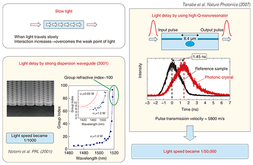
Front-line Researchers Vol. 9, No. 7, pp. 1–6, July 2011. https://doi.org/10.53829/ntr201107fr1  Toward the Ultimate in Optical Integration TechnologyPhotonic crystal, which can function as a photonic insulator (something not found in nature), is expected to provide major breakthroughs in optical integration technology. Dr. Masaya Notomi, Senior Distinguished Scientist at NTT Basic Research Laboratories, is a driving force behind research that aims to achieve on-chip optical networks by applying the special properties of photonic crystal. We asked him about his research experiences and what led him to take up the challenges of photonics.  Photonic crystal: achieving optical integrated circuits—Dr. Notomi, could we begin by hearing about the research that you are now pursuing? I am now researching the creation of structures called photonic crystals using nanofabrication techniques with the aim of developing optical large-scale integration technologies that have so far been difficult to achieve. A major objective of this research is to resolve problems in existing electronics technologies by introducing genuine photonic network technologies in information-processing chips. In electronic circuits, the more you raise performance the more you increase energy consumption and heat. In optics, however, increasing processing speed causes almost no increase in energy consumption. In other words, the energy consumption and heat generation can be minimized by introducing optics-based processing in circuits. With this in mind, researchers are attempting to incorporate optical wiring and circuits into electronic circuits using a variety of methods. To begin with, achieving large-scale integrated circuits by optical means inside a chip requires the fabrication of devices and wires (that is, optical waveguides) whose structures completely confine light. It also requires that the size of individual devices and wires be exceedingly small to achieve large-scale integration. In this regard, photonic crystal can function as a photonic insulator and confine light in a very small space, which makes it applicable to the fabrication of optical integrated circuits. By the way, although there are a number of naturally occurring insulators that block the flow of electricity, no photonic insulators exist in nature. The artificial structure of photonic crystal makes it possible to achieve photonic insulators for the first time. Furthermore, in the processing of signals for a logic operation in information-processing circuits, some packet signals must be made to wait until the others arrive so that the computation can be performed. To date, however, optical circuits have been incapable of making optical signals wait, and this has been one of their weak points. Photonic crystals, however, can significantly slow down the propagation speed of light. In the laboratory, we have been successful in using photonic crystal to produce extremely slow light with a speed about 1/50,000 that of ordinary light (Fig. 1).
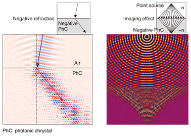
Photonic crystal has various peculiar properties in addition to slow light. One example is the phenomenon of negative refraction whereby the refractive index is made negative by using a special type of photonic crystal (Fig. 2). In the natural world, the refractive index is positive for all substances, but a negative value can lead to unexpected and interesting phenomena. For example, a simple flat surface can function as a lens if it has a negative refractive index.
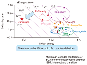
Ongoing innovation in optical technologies—What kinds of results is your research team currently aiming for? One use of photonic crystal that we have been thinking about is the development of ultralow-energy and ultrasmall high-performance optical devices for use in information-processing equipment. Up to now, the large amount of power consumed by microprocessor units (MPUs), for example, has prevented them from being incorporated into compact information-processing equipment such as mobile phones. The characteristics of electronic circuits inside MPUs are such that the energy cost of information transfer increases with the bit rate, which means that it is difficult to significantly reduce power consumption while raising processing capacity. However, if we could incorporate optical technologies into MPUs, the energy cost of information transfer would not increase for higher bit rates, which should make it possible to drive circuits by using much less power than in the case of electronic devices even as processing speed increases. In our research, we have already demonstrated that photonic crystal can be used to drastically reduce operating energy in a number of optical devices (Fig. 3).
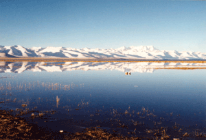
In addition to low power consumption, another requirement here is the integration of individual devices. Our aim is to develop optical integration technologies so that we can achieve optical integrated circuits while maintaining this energy-saving effect. Research on photonic crystals is still at the fundamental level, but we can expect optical integration technologies—if successfully developed—to be applied to commercial products sometime in the future. At the same time, high-precision photonic crystals will be needed to fabricate high-quality optical devices, and the key to this is the development of advanced fabrication techniques. Over the ten years that our team has been in existence, we have been making steady improvements in the performance of photonic crystal and have been working to improve our fabrication techniques. It is acknowledged that NTT has been able to fabricate high-quality photonic-crystal waveguides from an early stage because of these efforts. Establishing high-precision fabrication techniques is extremely important for later research. Looking back at the history of electronic circuits, we can see how vacuum tubes were followed by transistors and how technologies for integrating transistors on a chip were developed by Intel and other companies. In a similar way, innovations in optical technologies are now appearing one after another. Up to now, only individual optical devices could be developed, but their evolution toward integrated optical circuits is beginning. If fabrication techniques continue to progress, we can expect optical technologies to somehow be incorporated into chips in about ten years time. I believe that photonic-crystal technology will play an important role in this evolution. Adoption of a new theme and formation of a cross-organization team in caravan form—Could you tell us about the path that you took to your current research endeavors? During my university days, I researched the peculiar behavior of electrons confined to one-dimensional states by synthesizing crystals having a pseudo one-dimensional structure and cooling them to extremely low temperatures. Then, after joining NTT Laboratories in 1988, I undertook research on structures that could confine electrons to one-dimensional or even zero-dimensional states with particular application to optical devices. At that time, my superiors in this research group were being transferred, and in the end, I came to continue this research on my own. I was still just a new, young researcher, and there was not much of a budget, but upon looking back, I could say that this was a research environment that gave me much freedom. After performing this research for about ten years, I had written a number of papers and had completed enough research to write my doctoral thesis. It was at that time that my superior asked me what I thought about changing research theme. He was also very generous in telling me that “Whatever you do is fine so please select a new theme of your own choice.” I then spent about one year in Sweden as a visiting researcher during which time I completed my doctoral thesis and thought about my next research theme. Around that time, photonic crystal research was passing from the concept phase to the testing of operating principles using microwaves. While I was in Sweden, such testing in the optical wavelength region began. In Japan, photonic crystal research had begun only in some universities, but the worldwide number of researchers involved in this field was starting to climb. Moreover, the photonic crystals were relatively large structures with feature dimensions greater than 100 nm, which was about one order of magnitude larger than the structures that I had fabricated in past research. Such a large structure was technically easy to fabricate. Taking all of this into consideration, I decided that photonic crystals would be my next research theme. At that time, I also hatched a plan to shift from individual research as I had been doing to research that I would perform with fellow researchers. We called this our caravan plan in which we would recruit researchers with an interest in photonic crystals not only from the organization to which I belonged but also from other research laboratories. This does not mean to say that many researchers suddenly offered to participate, but people from several groups started to express interest and I was eventually able to form a cross-organization team. At NTT Laboratories, there is actually a lot of interdisciplinary research, but most of this involves the development of practical products over a two- or three-year period. Fundamental research themes like the one that we were pursuing with photonic crystals were actually quite rare. This cross-organization team was able to conduct research on photonic crystals using fabrication and measurement techniques that were not previously available, which I believe had a great effect on results. Pushing yourself into a state conducive to inspiration—Please tell us about your current research team. At present, there are seven members from the same research laboratory and several members from other laboratories. Our research on photonic crystals is broken down into several themes with several members dealing with each. Of utmost concern here is that each and every theme should be something that will grow over time. For this reason, I leave everyday research to team members, but I think about medium- and long-term research themes by forecasting the state of development several years in the future and then working backwards to the present. Looking for a theme on one’s own from a blank slate is certainly not unpleasant, but there is pressure just the same. And the fact is that, if you don’t push yourself into such a state, you cannot expect inspiration or novel ideas to form. Pushing oneself mentally, though, is not necessarily fun. When I find myself in such a situation, I think back to my experiences as a visiting researcher in Sweden, when I would think every day about what I should be researching. Those experiences are proving to be quite useful even today. I am also very grateful to my superior who gave me the time to ponder my next move. Research work, though, is often a matter of trial and error and also of detours as researchers grope for answers. Consequently, there must be some margin and flexibility in the time, people, and organizations specified for a research project to prevent researchers from coming to a standstill. In this regard, I think that researchers at NTT Laboratories are fortunate to be working in an environment conducive to basic research. Traveling to Tibet alone—Do you have any hobbies or interests outside of research? Yes, I do. After entering the workforce and while I was still single, I would often travel by myself to places overseas. I first travelled to popular destinations in North America and Europe, for example, but in time, I got bored with such trips, and I eventually started to visit countries like Tibet, India, and Vietnam. I thought that Tibet, in particular, was fascinating, and my trip to Lake Namtso (or Gnam-mtso) in the highlands of Tibet left a strong impression on me. This lake is located in a rural area several hundred kilometers from the capital; there are no roads leading up to it, so it cannot be accessed by normal modes of transportation. But wanting to go there, I gathered some information after arriving in Tibet, and I found that I could charter a jeep. The driver and I set out in the direction of the lake with no roads to go by. After much difficulty, we eventually arrived. I thought that Lake Namtso was too beautiful for this world. Situated at an elevation of 4718 m, it is the highest salt lake in the world. This lake is so magnificent that it is proudly called the “sacred lake” or the “lake nearest to heaven” in the Tibetan language (Photo 1).
After I got married and had children, my solo trips came to an end, but I still love to walk around town. On my days off, I often take my kids with me on walks to temples, art galleries, and other interesting places. Becoming a better researcher by understanding your research theme—Dr. Notomi, could you please leave us with some advice for young researchers? I would be happy to. First of all, it is helpful to have staying power over the long term with respect to one’s research theme. All researchers, myself included, can lose spirit if research results do not turn out as expected. But that’s when you must have the fortitude to withstand such painful periods and not give up. This is something that I tell myself all the time. Secondly, you must discover for yourself what it is about your research theme that is interesting or exciting. If you don’t develop on your own a deep understanding of the possibilities behind your research theme and what that theme might mean to the field in question, you will never discover just how interesting your research theme can be. And if you can’t discover that, you will not be able to continue your research over the long term. It is relatively easy to get a budget for research that is currently fashionable, and in recent years, even university students have been switching over to such research in great numbers. I guess some researchers are worried that they will be left behind if they don’t get on board immediately with such fashionable research. However, I feel that this kind of impatience in research can be very dangerous. This is because most of research is a series of failures, but that does not mean to say that there are no successes, few though they may be. Researchers must continue to research while accumulating the results of those successful experiments over time. Even if failures should continue, researchers that can discover on their own the fascinating aspects of their research should be able to use those experimental failures to get on a path toward success. In this way, researchers should be able to continue researching without getting discouraged even if successes are few and far between. In this sense, I believe that discovering what is exciting in your research by yourself is an important qualification for a researcher. Masaya NotomiSenior Distinguished Scientist, Group Leader, Photonic Nanostructure Research Group, NTT Basic Research Laboratories. He received the B.E., M.E., and Dr.Eng. degrees in applied physics from the University of Tokyo in 1986, 1988, and 1997, respectively. He joined NTT Optoelectronics Laboratories in 1988. Since then, his research interest has been to control the optical properties of materials and devices by using artificial nanostructures. He has been in NTT Basic Research Laboratories since 1999. During 1996–1997, he was a visiting researcher at Linkoping University in Sweden. He was a guest associate professor in the Department of Applied Electronics at Tokyo Institute of Technology (2003–2009) and is currently a guest professor in the Department of Physics at Tokyo Institute of Technology. He received the 2006–2008 IEEE/LEOS Distinguished Lecturer Award, JSPS (Japan Society for the Promotion of Science) Prize in 2009, the Japan Academy Medal in 2009, and the Commendation for Science and Technology from the Minister of Education, Culture, Sports, Science and Technology (Prize for Science and Technology, Research Category) in 2010. He is a member of the Japan Society of Applied Physics, the American Physical Society, the Optical Society of America, and IEEE. |