|
|||||||||||||||||||||||||||||||||||||||||||||||
|
|
|||||||||||||||||||||||||||||||||||||||||||||||
       |
Regular Articles Vol. 9, No. 8, pp. 73–78, Aug. 2011. https://doi.org/10.53829/ntr201108ra1 Ultralow-energy All-optical Switches Based on Photonic Crystal NanocavitiesAbstractPhotonic crystal cavities having a wavelength-sized volume exhibit a strong light-matter interaction, which makes possible all-optical switches operating with ultralow energy consumption. Using the combination of an extremely small photonic crystal nanocavity and strong carrier-induced nonlinearity in InGaAsP, we have successfully demonstrated low-energy switching in the attojoule range for the first time. This switching energy is more than two orders of magnitude lower than that of previously reported optical switches. The ultrasmall cavity also contributes to fast carrier diffusion and hence a fast switching response of 20 ps at minimum. These all-optical switches with their small size and low-energy, fast-response operation may open up the possibility of a dense photonic network on a chip. 
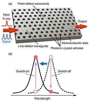
1. IntroductionPhotonics has played a key role in the progress of long-haul network links. On the other hand, although data processing at nodes or routers is still performed with integrated electronic circuits, their increasing power consumption and heat generation during high-bitrate operation is now becoming an obstacle to further improvements in network speed and traffic capacity. All-optical data processing with integrated photonic circuits is therefore expected to reduce the amount of power consumed by their electronic counterparts while keeping the high-speed properties of optical signals [1]. However, current photonic processing devices generally require a very high driving energy and are too big for integration, though future interconnect technology will demand micrometer-scale optical components in a chip consuming less than a femtojoule per bit [2]. These problems arise from the difficulty of confining light in a small volume and the weakness of light-matter interactions. Photonic crystal (PhC) cavities, which exhibit a high cavity quality factor (Q) and an ultrasmall modal volume (V), are promising candidates as platforms on which to construct devices with dimensions on the order of a few wavelengths of light in matter. Since optical nonlinearities can be greatly enhanced in high-Q, small-V cavities (the optical-field intensity is enhanced in proportion to Q/V), very low operating energy/power can be expected if we apply them to various functional devices. The all-optical switch, which enables gating of an optical signal, should be one of the fundamental elements for constructing photonic circuits [3]–[6], and it is a straightforward example of light-matter interaction enhancement by nanocavities [7]–[9]. A PhC nanocavity is schematically illustrated in Fig. 1(a). A two-dimensional array of airholes is patterned into a semiconductor thin plate having a thickness of ~200 nm. A line defect and a point defect in the array can act as an input/output waveguide and a nanocavity, respectively. The PhC nanocavity can strongly confine light, thereby achieving a strong light-matter interaction and optical nonlinear functionalities [10], [11]. The operating principle of all-optical switching is shown in Fig. 1(b). The pump and signal light pulses are injected into the waveguide simultaneously. The pump light generates carriers in the nanocavity and induces a wavelength shift in the resonant transmission spectrum, which makes it possible to control the signal light output. This article clarifies the design principle for a PhC-nanocavity-based switch, namely, what type of cavity, nonlinearity, and material we should use. Devices based on our designs exhibit all-optical switching with operating energy in the attojoule range and a time window of a few tens of picoseconds. Our results clearly show that PhC nanocavities enable unprecedented all-optical switches that may lead to high-speed, low-power information processing on a chip.
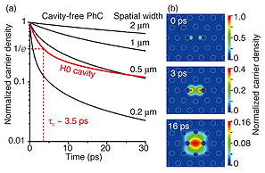
2. Design2.1 Smallest PhC cavityAlthough we said that a high Q/V ratio is preferable for a lower switching energy, that is a bit too simple. In practice, we need to choose an appropriate Q according to the target operating speed because the photon lifetime in a cavity is proportional to Q. In contrast, cavity volume V should always be as small as possible. In this study, we used a lattice-shifted cavity (hereinafter referred to as an H0 cavity) [12]. The cavity mode consists of only two primary antinodes (Fig. 2(a)). Importantly, the H0 cavity has the smallest V among dielectric-core PhC cavities. In our simulation, V was calculated to be only 0.025 µm3. Another limiting factor for operating speed is the carrier relaxation time (τc). Generally, τc is as long as the nanosecond order, but PhC nanocavities offer an efficient way to reduce it. When the cavity becomes ultrasmall, the photogenerated carriers rapidly diffuse out from the cavity, and τc becomes small [13]. We numerically solved the carrier diffusion dynamics in a PhC nanocavity. First, we investigated the carrier dynamics without a cavity but assuming an initial Gaussian carrier distribution centered at a certain point in a defect-free PhC lattice. In Fig. 2(a), four black lines show the decay for different initial distribution sizes. They clearly show that a small excitation leads to surprisingly fast diffusion. We investigated more realistic cases with an H0 cavity, as shown by the red line. The fitted tc values are as short as 3.5 ps. The time evolution of the carrier distribution for the H0 cavity is shown in Fig. 2(b). The carriers are initially localized in the cavity mode and then start to spread out. This result implies that we can expect a switching bandwidth of nearly 100 GHz. Consequently, it shows that an H0 cavity switch is promising in terms of high-speed response.
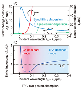
2.2 Material optimizationTo obtain lower switching energy, we want the pump light to be efficiently absorbed in the cavity and the subsequent refractive-index change to be large. InGaAsP is one compound semiconductor that exhibits these features effectively compared with other materials such as Si and GaAs at a wavelength of 1.55 µm. Figure 3(a) shows the calculated index change and the linear absorption lifetime as a function of the incident wavelength detuning from the bandgap wavelength λin – λg. In our switch, all-optical switching relies on band-filling dispersion (BFD) and free-carrier dispersion in InGaAsP to obtain a refractive index change [14]. Since BFD depends strongly on the position of the electronic band-edge wavelength, we need to find an appropriate InGaAsP composition to suit the cavity’s resonant wavelength. On the other hand, optical absorption relies on linear absorption (LA) and nonlinear two-photon absorption (TPA). LA also becomes stronger in the vicinity of the band-edge wavelength and allows efficient absorption. The important point is that excess absorption induces a degradation of cavity Q and increase in switching power, so appropriate adjustment of the composition is needed in order to minimize the switching energy. The calculated switching energy Usw for the H0 nanocavity is shown in Fig. 3(b). In the vicinity of the band edge, LA boosts the absorption efficiency and BFD enhances the nonlinear resonance shift, thereby effectively reducing Usw. This results in a minimum value of less than 1 fJ at around λin – λg = 0.05 to 0.1 µm. We adjusted the InGaAsP composition to set the photoluminescence peak to 1.47 µm for an operating wavelength of around 1.55 µm.
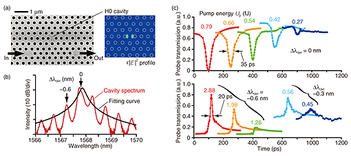
3. Switching demonstration3.1 Fabricated H0 nanocavityWe fabricated H0-PhC cavities in an InGaAsP slab using standard top-down processes, including electron-beam lithography and Cl2-based dry etching. A top-view image of the device is shown in Fig. 4(a). The air-hole diameter, lattice period, and slab thickness are 230, 460, and 200 nm, respectively. The H0 cavity, which was formed by shifting two neighboring air holes by 85 nm in opposite directions, is coupled with input and output PhC waveguides. The transmission spectrum acquired by scanning a wavelength of continuous-wave light is shown in Fig. 4(b). The periodic peaks in the spectrum are not a nanocavity mode, but appear as a result of interference with the Fabry-Pérot resonance caused by the facet end of the waveguide. The fitting curve (black) clarifies the nanocavity mode, indicating that the resonant wavelength λcav and linewidth are 1567.8 nm and 0.24 nm, respectively. The cavity Q factor is 6500 and the corresponding photon lifetime is τph = 5.4 ps, which is slightly longer than the calculated carrier relaxation time of 3.5 ps and is thus unlikely to restrict the switching recovery time. 3.2 Pump-probe measurementTo measure the switching dynamics, we used a degenerate pump-probe technique with an optical pulse width of 14 ps [7], [15]. The center wavelength of the pump pulse was always set to the resonance wavelength, while the wavelength of the probe pulse λprobe was set with detuning Δλdet = λprobe – λcav. Switching dynamics for different values of Δλdet are shown in Fig. 4(c). For Δλdet = 0.0 nm, the transmission of the probe pulse was abruptly switched off when the pump pulse temporally overlapped the probe pulse. On the other hand, the probe transmission was switched on for Δλdet = –0.3 nm and–0.6 nm because pump-induced carrier nonlinearity induced a resonant blueshift. Switching energies of 420 and 660 aJ were achieved for contrasts of 3 and 10 dB, respectively. These energies are over two magnitudes lower than those reported for Si- and GaAs-based PhC cavities. It should be noted that the switching time window is only 20–35 ps. This value is much shorter than the carrier recombination lifetime (several hundred picoseconds), which is attributable to the rapid carrier diffusion. The improvement in energy and speed is attributed to the ultrasmall size of the cavity and the strong nonlinearity of InGaAsP.
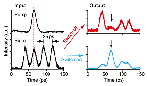
3.3 Gate switching for 40-Gbit/s signalWe performed an experiment in which we extracted a pulse from a repetitive signal train to demonstrate the practicality of our all-optical switches. As shown in Fig. 5, we generated a signal train with four pulses with a 25-ps period (40-Gbit/s repetition). We also injected a pump pulse so that it temporally overlapped the second signal pulse to switch it selectively. Output signal pulses show the result of the pulse extraction experiment; they indicate that the second pulse (indicated by an arrow) was selectively switched off or on. These results are promising in terms of the suitability of PhC nanocavity switches for 40-Gbit/s operation.
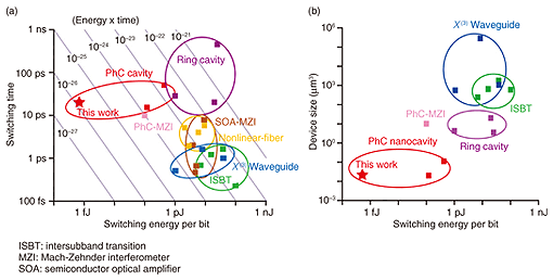
4. Comparison of all-optical switchesVarious all-optical switches are compared in Fig. 6(a) in terms of their switching energy per bit and switching time. It is clear that our switch can operate with energy approximately two or more orders of magnitude less than for previously reported ones and has entered the attojoule energy range for the first time. In addition, the previous all-optical switches suffer from a trade-off between switching time and energy; that is, the energy-time product is limited to around 10–24–10–22. On the other hand, our device clearly overcomes this limitation, exhibiting an energy-time product of 10–26. This is attributed to the ultrasmall size of our cavity. On-chip all-optical switches are compared in Fig. 6(b) in terms of switching energy and device size. Our device exhibits both the smallest size and lowest energy. Although all-optical switches involving third-order nonlinearity [16] and inter-subband transition [5], [6] can operate at a much higher bitrate, their high energy consumption and large size might be unacceptable for an on-chip integrated circuit. With our device, assuming 1000 devices on a single chip all operating at a bitrate of 10 Gbit/s, the power consumption is only a few milliwatts. In addition, the ultrasmall size of our device lets us integrate 1000 devices with a small footprint of less than 0.01 mm2 (assuming a footprint for a single device of less than 10 µm2). Consequently, the low-power, ultrasmall, and fast PhC-nanocavity switch studied here is unique.
5. ConclusionWe demonstrated all-optical switching with extremely low power consumption using a PhC nanocavity. The achievement of such a densely integrable PhC-nanocavity switch is very important because it will enable low power consumption in the milliwatt range, even in an integrated chip including thousands of devices with a sub-mm2-order footprint, and it operates at 40 Gbit/s. A wide variety of low-power optical devices, such as optical bistable memory and logic elements [17], [18], should be achievable in a similar way. These PhC-nanocavity-based functionalities are promising for use in optical processing in chip-scale photonic integration. AcknowledgmentsWe thank Dr Toshiaki Tamamura of Nano F Consultant (Japan) for help with sample fabrications. This work was partly supported by Core Research for Evolutional Science and Technology (CREST) of the Japan Science and Technology Agency (JST). References
|
||||||||||||||||||||||||||||||||||||||||||||||