|
|||||||||||||||||||||||||||||||||||||||||||||||||||||||||||||||||||||||||||
|
|
|||||||||||||||||||||||||||||||||||||||||||||||||||||||||||||||||||||||||||
       |
Regular Articles Vol. 9, No. 12, pp. 42–52, Dec. 2011. https://doi.org/10.53829/ntr201112ra1 Power-management-circuit Techniques for Low-power Intermittent LSI Operation in Wireless ApplicationsAbstractPower-management-circuit techniques for low-power intermittent LSI (large-scale integrated circuit) operation are discussed for various wireless transceiver designs. For an RFID (radio-frequency identification) application, the most important issue is reducing the power of the clock timer; we used an analog RC (resistor-capacitor) timer circuit with megaohm resistors. For a sensor node that has a power generator, the ability to operate with a nanowatt-level power supply is essential; we devised a two-stage power management circuit with a subnanowatt voltage-detection circuit. For wide-area-ubiquitous-network transceivers, the power-management circuit should supply 100 mA of current in the active mode and reduce the leakage current to the nanoampere level; we developed a regulator circuit with a reversely biased nMOS/pMOS cascode switch to reduce the leakage current and with a DC-DC converter for supplying sufficient current without any increase in power consumption. 
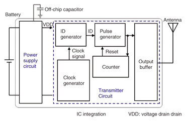
1. IntroductionThe number of wireless applications using small terminals, such as the wide area ubiquitous network (WAUN [1]–[2]), wireless sensor networks [3]–[6], and active RFID (radio-frequency identification) [7]–[12], has been increasing. Small wireless terminals must have very low power consumption and small power supplies such as coin batteries or small power generators [3]–[6]. In such wireless systems, intermittent operation is one of the key techniques for reducing the power consumption of the terminals [13], [14]. The average power consumption of the terminals can be reduced by decreasing the activity ratio of the intermittent operation. However, the method of controlling intermittent operation varies depending on the power consumption of the transmitters, preciseness of the transmission timing, power supply capabilities, and so on. In this article, we describe power-management-circuit techniques for low-power intermittent LSI (large-scale integrated circuit) operation in power-management-circuit designs for three different applications: RFID devices, sensor nodes, and WAUN transceivers. For RFID, the most important issue is reducing the power of the clock timer; for this purpose, we use an analog RC (resistor-capacitor) timer circuit with megaohm resistors, all-digital RF transmission, and automatically tuned RF pulse generation [15]–[17]. For an ultrasmall sensor node, a nanowatt-order power supply is essential; we have made one by using a two-stage power management circuit with a subnanowatt voltage detection circuit [18]–[24]. For WAUN transceivers, the power-management circuit must be able to supply 100 mA of current in the active mode and reduce the leakage current to the nanoampere level; we have developed regulator circuits with a reversely biased nMOS/pMOS (positive/negative-type metal oxide semiconductor) cascode switch to reduce the leakage current to the nanoampere level and with a DC-DC converter to supply sufficient current without any increase in power consumption [25], [26]. Our techniques for these applications are described in sections 2–4, respectively. 2. Micro-power active-RFID LSIFor an RFID application, the power-supply circuit usually has a timer clock (or processor) and provides power to the transmitter intermittently. However, a timer circuit that uses a crystal oscillator consumes a considerable amount of power. Our power reduction solution uses an analog RC timer circuit with megaohm resistors. Battery voltage fluctuations are stabilized through the use of all-digital RF transmission and automatically tuned RF pulse generation; as a result, the integrated circuit (IC) is suitable for practical use. A block diagram of the active RFID IC is shown in Fig. 1. The IC is divided into two major blocks: a power-supply circuit block and a transmitter circuit block. The battery and antenna are external components. The power-supply circuit controls the transmitter’s power and its on and off states. When power is provided by the power supply circuit, the transmitter starts to operate and it sends the device’s ID (identification) to a receiver.
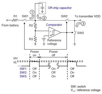
The architecture of the power-supply circuit, which consists of three switches, a comparator, and an off-chip capacitor, is shown in Fig. 2. Initially, switches SW1 and SW3 are on, and SW2 is off. The energy from the battery is stored in a storage capacitor to obtain a sufficient voltage level for transmitter operation. The comparator senses the change in the level and compares it with a reference voltage. When the voltage reaches the high threshold voltage (VH) level, the comparator turns on SW2 and turns off SW1 and SW3. Then DC power is provided to the transmitter from the capacitor, and the circuit starts to operate and it sends the ID. During this operation, the energy stored in the capacitor is consumed and the capacitor’s voltage level decreases. When the voltage reaches the low-threshold-voltage (VL) level, the comparator turns off SW2 and turns on SW1 and SW3. The battery starts to recharge the capacitor. At this point in the timing, the transmitter immediately stops operating because SW3 shorts the VDD (voltage drain drain) line to ground. This prevents unstable IC operation by avoiding operation at an insufficient voltage. This cycle is repeated until the battery runs down. This intermittent operation is effective for achieving a long lifetime in an active RFID tag. The typical operating voltage of an external battery is 3.4 V. VH and VL are 2.1 and 1.9 V, respectively. The total average current drawn from the battery is 1.6 μA. The comparator and voltage-reference circuit are the only components operating continually in the IC, and they consume about half the total average current.
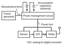
3. Nanowatt wireless sensor nodesWireless sensor nodes can be powered by small batteries (e.g., coin batteries) or small power generators. One popular approach is energy harvesting, in which energy is captured from external sources such as solar power, thermal energy, or kinetic energy (e.g., movement of a human body carrying the sensor). For a sensor node with a power generator, one of the most important issues is size reduction: sensor nodes as small as dust grains are expected [5]. However, the amount of power that a power generator can generate is almost proportional to its size [6]. Dust-sized sensor nodes must operate with nanoampere-level power generators [18]–[24]. Since the generated power is much less than that needed for radio transmission, the generated energy must be accumulated by the sensor node until it has enough for a transmission burst (intermittent operation) [3]. However, since the power management circuit runs continuously not intermittently, the power management circuit’s power consumption cannot exceed the generated power. Thus, the power management circuit, which monitors the accumulated energy and controls the current flowing into the radio block, is a key circuit affecting the minimum current that must be accumulated. The target sensor-node architecture is depicted in Fig. 3. The architecture has four key elements: a power generator, power management circuit, vibration sensor, and radio block. The sensor nodes should be smaller than 1 mm3 [6]. Thus, the power generator outputs nanowatt-level power and the power management circuit accumulates that energy in capacitors. When enough energy to operate the radio has been accumulated, the power management circuit supplies power to the sensing circuit, analog-to-digital converter, and radio block.
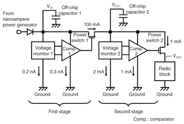
For a design in which energy from a generator is accumulated and supplied to the radio block, there are two issues to resolve. One, as mentioned above, is that the total power consumption of the power management circuit must be less than the generated power. The total power consumption consists mainly of the power consumed for monitoring the voltage and controlling the switches and the leakage current flowing through the power switch transistor. The other issue is that the transition time of the power switch should be sufficiently shorter than the operation time of the radio block. This is because the output voltage of the management circuit is too low for radio operation during the transition period, so during this period the output power is wasted. Such waste should be minimized so that most of the accumulated energy is used for radio operation. A simulation showed that the sum of the switch leakage current and comparator current is 19 nA for a pMOS switch or 11 nA for an nMOS switch [24]. Since these values are both greater than 1 nA, a single-stage power management circuit cannot accumulate energy from a nanoampere power generator. Therefore, we designed a two-stage power management architecture, as shown in Fig. 4. This architecture can resolve both of the issues described above. The first stage accumulates the energy from a nanoampere power generator and supplies about 100 μA of current to the second stage. The second stage accumulates the 100-μA current from the first stage and supplies about 1 mA of current to the radio block.
The voltage-monitoring circuit in the first stage is shown in Fig. 5. The current consumption of the first stage must be much lower than that of the second stage because the first stage must operate continuously whereas the second stage operates intermittently. With a previously proposed technique, the low-power band-gap reference circuit consumes about 0.2 µW [27]; therefore, the remaining available power is too low to enable the power management block to operate with nanowatt-level power. This is because calculations based on Ohm’s law show that the resistors in the band-gap reference circuit operating at a voltage of 2 V would need to be more than 10 GW for subnanoampere operation. 10-GW resistors would require several square centimeters of chip area, which would be almost impossible in the available area on the chip.
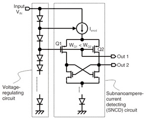
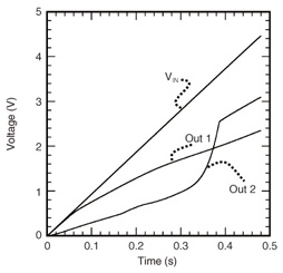
A subnanoampere-current-detecting (SNCD) circuit is used for the voltage-monitoring circuit in the first stage, as shown in Fig. 5. The voltage-monitoring circuit features subnanoampere operation, with voltage regulation through a series-connection of diode-connected MOS field-effect transistors (MOSFETs) and with positive-feedback amplification due to a cross-coupled transistor pair. The diode-connected MOSFETs in the voltage-regulating circuit are six pMOSFETs and three nMOSFETs; those in the SNCD circuit are three nMOSFETs. The threshold voltages of the pMOSFETs and nMOSFETs are -0.33 V and 0.30 V, respectively. The simulated transition characteristics of the input voltage VIN and the outputs of the voltage-monitoring circuit in the first stage (Out 1 and Out 2) are shown in Fig. 6. The input voltage VIN is the voltage of the accumulated energy. Initially, the diode-connected MOSFETs are in the off state. When VIN applies the threshold voltage to each diode, a subnanoampere current is generated in the voltage-regulating circuit. This current is mirrored to the current source Isncd in the SNCD circuit. This causes a current difference in MOSFETs Q1 and Q2 in the designed channel width: WQ2 > WQ1 (Fig. 5). This current difference is amplified and converted into a voltage signal by the cross-coupled transistor pair and the relationship between voltages Out 1 and Out 2 is inverted. This differential signal from the voltage-monitoring circuit is converted into a pulse by the hysteresis comparator, which means that the voltage of the accumulated energy reaches the voltage determined by the number of diode-connected MOSFETs. Thus, our circuit can monitor the voltage of the accumulated energy and regulate it using low power consumption at a subnanoampere current.
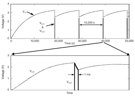
The simulated transition characteristics of the subnanoampere two-stage power management circuit are shown in Fig. 7. The input voltage VIN, the first supply voltage VDD1, and the second supply voltage VDD2 were evaluated at the points depicted in Fig. 4. In the simulation, the input current was 1 nA and the values for the first and second off-chip capacitors were 2.2 μF and 0.7 μF, respectively. The interval between intermittent bursts of the final accumulated output (VDD2) was about three hours. Our on/off keying (OOK) transmitter [15]–[17] can transmit 1000 bits of data using the VDD2 output.
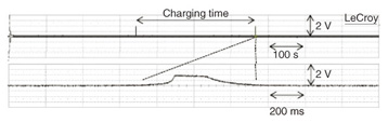
To confirm the effectiveness of our circuit techniques, we fabricated a test chip using the 0.35-μm complementary MOS (CMOS) process. To evaluate the characteristics of the voltage-monitoring circuit, we measured the time taken to charge the 2.2-μF accumulation capacitor by using a DC current source. Charging time was obtained from the waveform in Fig. 8. In this measurement, DC current of 1 nA was input to the rectifier, and the voltage at the measurement point of the switch controlled by the voltage monitoring circuit (VDD1 in Fig. 4) was measured with a digital oscilloscope having impedance of 1 MW. The accumulation capacitance was chosen to be 2.2 μF, which is the amount necessary to operate our OOK transmitter for one data transmission. The period of the measured pulse corresponds to the charging time, as shown in the upper waveform.
In Fig. 9, the solid line shows the measured charging time for our power management circuit, which includes a voltage detection circuit, and the dashed line is the calculated charging time for a previously reported voltage detection circuit [27]. If this previous circuit is used, the accumulation capacitor cannot be charged when the generated current is less than 0.1 μA. On the other hand, for our circuit, the accumulation capacitor can be charged with a 1-nA current, which corresponds to a solar cell less than 0.1 mm3 in size when the solar energy density is 10 μW/cm3. This means that the size of the power source needed for our circuit is 1/100 of that for the circuit in [27].
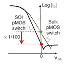
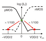
4. WAUN transceiversTerminals used in a WAUN must have small power supplies. To reduce power consumption, the wireless terminals operate intermittently with a very low activity ratio. Power reduction with a very low activity ratio strongly depends on power consumption in the standby mode. Thus, we use two key techniques for reducing the standby current: a special power switch for low leakage current and a minimized number of active blocks in standby mode. The standby current of the terminals is less than 5 μA, which is about 1/100 of that for other applications, such as ZigBee and PHS (personal handy-phone system). One of the most important circuits for low-standby-current performance is a power switch that can supply 100 mA in the active mode and reduce the leakage current to the nanoampere level in the standby mode. The off-state leakage current of MOSFETs is determined mainly by the subthreshold leakage, gate-induced drain leakage, and junction leakage currents [28]. MOSFETs based on semiconductor-on-insulator (SOI) technologies have a smaller subthreshold swing and smaller junction area than those based on bulk technologies. Thus, the subthreshold leakage and junction leakage currents of power switches can be aggressively reduced by using SOI technologies [29]–[30]. The voltage between the gate and source (gate-source) voltage dependences of the off-state leakage current with a constant drain-source voltage for pMOS power switches using SOI and bulk technologies are illustrated in Fig. 10. The leakage current of SOI MOSFETs at the gate-source voltage of 0 V is about 1/100 that of bulk MOSFETs. This means that just using SOI technologies can reduce the leakage current satisfactorily.
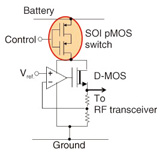
The architecture of the power switch and regulator circuits with CMOS/SOI technology is shown in Fig. 11. The power switch has a conventional architecture and consists of two pMOSFETs. A depletion-mode n-MOSFET (D-MOS) is used in the regulator circuit. This transistor has a negative threshold voltage and can control a large current by means of a low gate-source voltage, so it is useful for supplying stable current when the available battery voltage is low. A stable current supply requires an applied voltage that is sufficiently higher than the threshold voltage between the transistor’s gate and source. This is difficult to achieve if the source voltage is low and the threshold voltage is positive, but easy if the threshold voltage is negative.
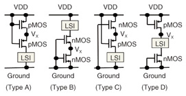
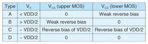
The standby-mode biases of four types of power switches are illustrated in Fig. 12. In each power switch, two transistors are connected in a cascode configuration. The gate biases of the nMOSFET and pMOSFET are the ground level and power-supply level, respectively. The intermediate potential (VX) values of the power switches are chosen to ensure that the leakage currents of the cascode transistors are equal. In a type-A power switch, the gate-source voltage of the upper pMOSFET is 0 V and that of the lower pMOSFET is more than 0 V. Thus, the VX value exceeds half of VDD. Similarly, the gate-source voltages (VGS) and VX values of type-B, -C, and -D switches can be estimated; the values are given in Table 1. From the conditions and values in Table 1, the type-C power switch is expected to have the lowest leakage current among the four power-switch architectures. This is because the gates of both transistors are reversely biased (i.e., the gate-source voltage of the upper nMOSFET is less than 0 V and that of the lower pMOSFET is more than 0 V) and the VX value is about half of VDD. Furthermore, the leakage current is expected to be aggressively reduced compared with the other power switches, as shown in Fig. 13.
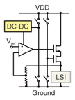
A typical architecture of a bulk regulator circuit with the new power-switch configuration is depicted in Fig. 14. An enhancement-mode nMOSFET is used for a power switch between the LSI and VDD. Thus, the voltage drop* across the nMOSFET is larger than the transistor’s threshold voltage because the voltage drop is equal to its gate-source voltage. This voltage drop is a big problem for low-voltage operation. Therefore, we use a DC-DC converter to raise the gate bias of the nMOSFET. The maximum gate bias of the nMOSFET is designed to be about twice the value of VDD in the active mode. On the other hand, the gate bias of the pMOSFET is fixed to the ground level. As a result, the regulator can supply sufficient current with a low battery voltage in the active mode.
Since the DC-DC converter is used only for the regulator circuit, a small converter is sufficient for this application. The small DC-DC converter operates only in the active mode. Thus, it does not increase the average power consumption of a regulator that has a low activity ratio. The leakage current in the standby mode is reduced by the new power switch in the main current path and by small switches in the regulator control paths. The gate width of the small switches is a thousand times smaller than that of the power switch in the main path. Thus, the total leakage current is not increased by the small switches in the regulator control paths.
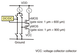
The maximum supply current and leakage current of the new power switch were measured using a TEG (test element group) circuit. The TEG architecture is shown in Fig. 15. The DC-DC converter makes the gate bias of the nMOSFET twice VDD in the active mode and zero in the standby mode. The gate bias of the pMOSFET is zero in the active mode and VDD in the standby mode. Currents in main path I1 and control path I2 can be measured individually.
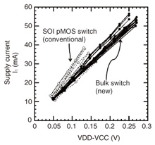
The measured current characteristics of I1 are shown in Fig. 16. The horizontal axis is the voltage drop across the power switches and the vertical axis is supply current I1. For comparison, the supply current characteristics of conventional SOI pMOS switches are also shown. The gate widths of the pMOSFETs and nMOSFETs of the switches were 900 µm and 600 μm, respectively. The gate length for both was 1.0 μm. From the data, we see that the supply current of the new bulk switches is almost the same as that of the SOI switches and that the supply-current characteristics of the former are more stable than those of the latter with respect to process variation.
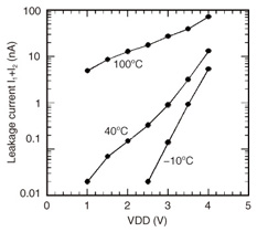
The leakage current versus VDD characteristics of the TEG measured at 100°C, 40°C, and -10ºC are shown in Fig. 17. The leakage current is the sum of the main path current I1 and control current I2. The max-imum voltage for VDD is 4 V. The leakage current of the new bulk switch is always lower than 100 nA in the graph’s temperature and voltage ranges.
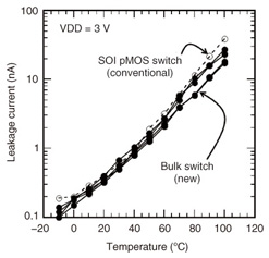
The measured leakage current versus temperature characteristics of the TEG at VDD = 3 V are shown in Fig. 18. The open plots are measured data for the conventional SOI MOS switch and the closed ones are for the new bulk switches. The temperature dependence of the leakage current is almost the same for the new bulk switch and conventional SOI switch in this temperature range.
5. ConclusionPower-management-circuit techniques for low-power intermittent LSI operation were described. Since they depend strongly on the wireless applications, three typical wireless applications were presented as circuit examples. These circuit techniques—an analog RC timer circuit with megaohm resistors, a two-stage power management circuit, and a new regulator circuit, individually or in combination, enable the supply of current ranging from 1 mA to 100 mA and can cut the leakage current to the sub-nanoampere level. Therefore, they are applicable to almost all low-power wireless terminals. References
|
||||||||||||||||||||||||||||||||||||||||||||||||||||||||||||||||||||||||||