|
|||||||||||||||||||
|
|
|||||||||||||||||||
       |
Regular Articles Vol. 10, No. 11, pp. 63–69, Nov. 2012. https://doi.org/10.53829/ntr201211ra1 512 × 512 Port 3D MEMS Optical Switch Module with Toroidal Concave MirrorAbstractWe present a 512 × 512 MEMS (microelectromechanical system) optical switch module in a W-shaped layout with a toroidal concave mirror. The 512-array optical components are made by assembling four 128-array components. The concave mirror minimizes the tilt angle of the MEMS mirrors. All of the optical path connections were demonstrated in a prototype module.
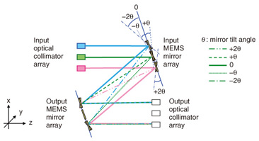
1. IntroductionAn all-optical cross connect will be a key component of large-capacity photonic networks and datacenter networks with low power consumption because it provides large-scale switching without optical-to-electrical-to-optical (O-E-O) conversion. A promising way to make large-scale optical cross connects (OXCs) is to use three-dimensional (3D) microelectromechanical system (MEMS) optical switches because of the potentially large port count and the compact configuration that can be achieved using free-space optics [1]. A 3D MEMS optical switch basically consists of a pair of optical collimator arrays as the input and output (I/O) ports and a pair of two-axis MEMS tilt mirror arrays to steer the optical beams so that any input port can be connected to an arbitrary output port. We previously reported a 100 × 100 port 3D MEMS optical switch module that provides good switching characteristics [2]–[4]. In this article, we describe a large-scale optical switch with a port count of over 500 and confirm the scalability of 3D MEMS optical switches. 2. Principle and designWhen the port count exceeds a few hundred, the requirement for the maximum tilt angle of MEMS mirrors becomes exacting because of the expanded connection area. A cross-sectional view of the optics in a conventional 3D MEMS optical switch is schematically shown in Fig. 1. The I/O ports and a pair of MEMS mirror arrays are arranged in a Z-shaped layout. In this configuration, the maximum tilt angle for switching depends on a mirror’s position in the array.
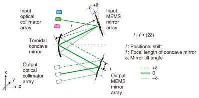
For example, let us denote by θ the angle that the central mirror needs to tilt by (dashed and dotted green lines). In that case, the mirror at the corner of the input MEMS mirror array connects to the opposite corner of the output MEMS mirror array when its tilt angle is 0° (solid blue line); however, it must tilt to one side on each axis with the maximum angle 2θ to connect to the diagonally opposite corner of the output MEMS mirror array (dot-dashed blue line). This position dependency makes the required maximum tilt angle excessively large. One way to keep the tilt angle from increasing is to apply an optical Fourier transform between the two mirror arrays to make the required tilt angle the same for all the mirrors [5]. We use a toroidal concave mirror as the optical Fourier transform element. A concave mirror also enables a compact W-shaped layout with a folded optical path. Another problem is how to produce large-scale optical components. As the array scale is increased, the process yield decreases significantly owing to the difficulty of fabrication. To solve this problem, we chose to use a 2 × 2 array of 128-port optical units to obtain a 512-port optical component. This achieves high fabrication yields with a small accumulated pitch error. 2.1 Basic switch structureA cross-sectional view of the configuration of our 512 × 512 port 3D MEMS optical switch module is shown in Fig. 2. The input and output MEMS mirror arrays are placed on the concave mirror’s two focal planes.
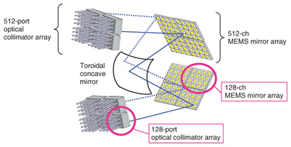
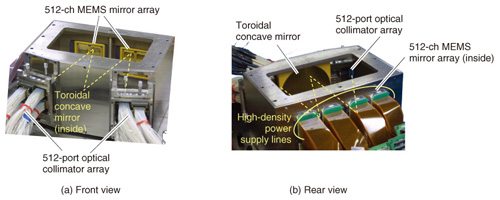
An optical beam deflected by an input mirror strikes the concave mirror at an incident angle that is related to the mirror’s tilt angle δ. The concave mirror provides a Fourier transform, causing the optical beam to converge onto the output mirror array with a positional shift l. The angle of each output mirror is adjusted so that the beam is reflected into the proper output collimator. The shift l is expressed by using the concave mirror’s focal length f as l=f · 2δ. This expression means that the connecting output mirror is determined by the input mirror’s tilt angle, without positional dependence in the mirror array. Thus, the increase in the maximum tilt angle of the MEMS mirrors is minimized throughout the mirror array. Folding the optical path into a W-shaped configuration enables a compact layout, but it also introduces the off-axis aberrations of the concave mirror in the x-z plane. We chose a toroidal surface for the concave mirror’s geometry to reduce the aberrations. For the optimized mirror geometry, the calculated loss due to aberrations is below 0.5 dB. A schematic of our 512 × 512 port 3D MEMS optical switch module is shown in Fig. 3. The mirror and collimator arrays consist of 2 × 2 arrays, each handling 128 ports. The 128-port optical components provide high fabrication yields with a small accumulated pitch error.
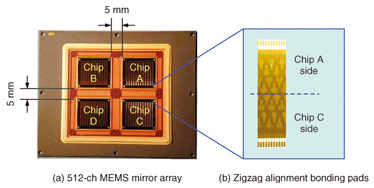
2.2 512-channel MEMS mirror arrayThe 512-channel MEMS mirror array is shown in Fig. 4. It contains four 128-channel MEMS mirror array chips, which are precisely mounted in a ceramic package by multichip-module technology. The positioning accuracy of mounting is less than 50 µm.
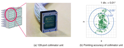
While the huge number of bonding pad electrodes should be assembled in a package, a compact ceramic package is needed to expand the possibility of the optical layout design. Our high-density bonding pads in a zigzag arrangement minimize the package size to 76 mm × 90 mm and the spacing between adjacent chips to 5 mm. The increase in mirror tilt angle needed to accommodate this spacing is only 0.6°. The 128-channel mirror array chip has a two-dimensional (2D) arrangement of two-axis MEMS tilt mirrors. Each mirror has a gimbal structure that allows the mirror to rotate around two orthogonal axes [4]. The mirror is actuated electrostatically by four electrodes underneath it, resulting in a tilting range of 4.5° in any arbitrary direction. 2.3 Optical collimator arrayThe 512-port optical collimator array is also composed of four 128-port units. They are mounted on a frame with a positioning mechanism that helps align them with the mirror array. Each collimator array unit consists of an array of 128 fibers and an array of 128 microlenses, as shown in Fig. 5(a).
The 128-port fiber array is made by inserting optical fibers with microferrules through a polymer substrate having precisely aligned holes. Each optical fiber is attached to a microferrule that had its end facet polished and antireflection-coated before assembly. This fabrication method is advantageous to improve the yield of a large-scale, highly accurate fiber array inexpensively [6], [7]. The 128-port microlens array is fabricated by a precise molding method using transparent optical polymer material. Both surfaces of the microlens array are also antireflection coated to reduce multiple reflections. The fiber array and microlens array are passively aligned using dowel pins with an accuracy of ±1 µm. The mean pointing accuracy, which is the mean angular deviation caused by a lateral offset of the axis of a microlens from that of the corresponding fiber, is 0.03°. The uniformity of our optical collimator’s pointing accuracy is shown in Fig. 5(b). This is adequate for good optical coupling. 2.4 Switch module assemblyFor switch module assembly, the critical issues are precise alignment and the assembly procedure itself: both are time consuming and costly. To reduce the cost, we use passive assembly to construct the optical system. A prototype 512 × 512 port switch module is shown in Fig. 6. The module size is 197 mm × 243 mm × 140 mm. All components are passively mounted on the housing by using dowel pins and holes. Before the concave mirror is set in the housing, the collimator arrays are visually aligned to the corresponding MEMS mirror arrays by observation using an infrared camera.
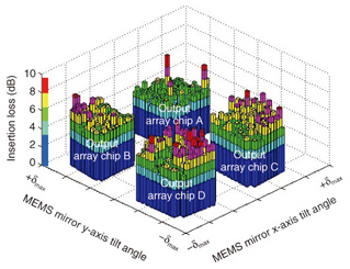
3. Optical performance of the switch moduleRegarding the optical performance, we measured the insertion loss of all the paths. A fast peak search algorithm enables accurate optical path connections at short measuring times [8]. The characteristics of the optical connections from an input mirror to all the output mirrors are shown in Fig. 7. This input mirror was located in the top-left corner of the array, which is at the maximum off-axis position. The vertical axis is insertion loss, and the horizontal axes are the tilt angles of the input mirror about the x- and y-axes. The maximum tilt angle is the same for both axes. The variation in mean insertion loss for the four output MEMS chips was less than 1 dB, which means that there were no significant differences among them. We also found that the characteristics of all the optical connections were roughly uniform.
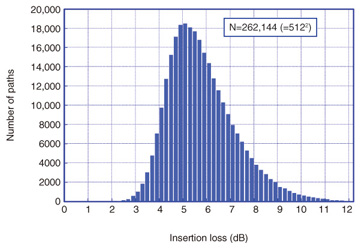
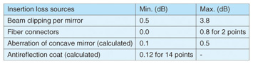
The distribution of the insertion loss for all the paths of the prototype module is shown in Fig. 8. The number of paths is 262,144 (i.e., 5122). The mean fiber-to-fiber insertion loss is 5.3 dB. A breakdown of the insertion loss sources is given in Table 1. The main one is clipping by the MEMS mirrors. The misalignment of a collimator caused a maximum beam position error of 250 μm, which is equivalent to a clipping loss of 3.8 dB per mirror. It should be possible to reduce the misalignment to less than 50 μm by improving the assembly accuracy. This should reduce the maximum clipping loss to less than 1.5 dB.
4. ConclusionsWe have presented a free-space 512 × 512 port 3D MEMS optical switch module featuring a W-shaped optical configuration with a toroidal concave mirror. This configuration keeps the increase in the maximum tilt angle of the MEMS mirrors small. We also devised 512-port optical components, each consisting of four 128-port units. This design provides both a large port count and a low cost. The results of optical path tests on a prototype switch module show its feasibility for constructing a large-scale optical switch with a port count of over 500. References
|
||||||||||||||||||