|
|||||||||||||||||||||||||
|
|
|||||||||||||||||||||||||
       |
Regular Articles Vol. 11, No. 2, pp. 48–53, Feb. 2013. https://doi.org/10.53829/ntr201302ra1 Mechanical Transfer of GaN-based Devices Using Layered Boron Nitride as a Release LayerAbstractNitride semiconductors are the preferential choice in various device applications such as optoelectronics and high-power electronics. These gallium nitride (GaN)-based device structures can be grown on sapphire, silicon carbide, and silicon substrates, but not on large, flexible, and affordable substrates such as polycrystalline or amorphous substrates. This article reports our research results that demonstrate that hexagonal boron nitride (h-BN) can form a release layer that enables the mechanical transfer of GaN-based device structures onto foreign substrates. Aluminium (Al) GaN/GaN hetero-structures and indium (In)GaN/GaN multiple-quantum-well (MQW) structures grown on h-BN-buffered sapphire substrates, ranging in area from 25 mm2 to 4 cm2, were mechanically released from the host substrates and successfully transferred onto other substrates. The electroluminescence intensities from the transferred light-emitting diode (LED) were comparable to or higher than those from a conventional LED on a low-temperature AlN buffer layer, indicating that the MQW preserved its original quality after the transfer.
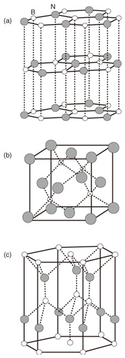
1. Introduction1.1 GaN semiconductor growthGallium nitride (GaN)-based semiconductors have a wide range of applications such as high-power devices for wireless communications, visible light sources for illumination, and ultraviolet light sources for sterilization. In general, GaN-based semiconductors have been grown on single-crystal sapphire substrates using a buffer layer, which can consist of low-temperature aluminium nitride (AlN) [1], low-temperature GaN [2], or aluminium oxynitride (AlON) [3]. However, high-quality GaN-based devices cannot be grown on polycrystalline or amorphous substrates even by using state-of-the art growth technologies such as metal-organic vapor phase epitaxy (MOVPE). The laser lift-off technique [4] enables the transfer of GaN-based devices from one substrate to another. However, it has some disadvantages, such as the need for laser lift-off equipment and a surface cleaning process to remove material residues after laser irradiation. Hence, there is a compelling need for a simple technique that requires neither chemical treatment nor additional equipment for the transfer. 1.2 Boron nitride as a release layerBoron nitride (BN) is not a naturally occurring chemical compound; it was first synthesized by W. H. Balmain [5] in 1842. This compound has three main crystal structures: hexagonal boron nitride (h-BN), cubic boron nitride (c-BN), and wurtzite boron nitride (w-BN), which are respectively shown in Figs. 1(a), (b), and (c). C-BN has been extensively studied for high-temperature and high-power applications. W-BN has a metastable crystal structure. H-BN, whose crystal structure is graphite-like with lattice constants of a = 2.50 and c = 6.66 Å, is a promising material for optical device applications in the deep ultraviolet spectral region. In addition, h-BN can potentially act as an ideal layer for mechanically releasing GaN-based devices from substrates because the layers in h-BN are bonded to each other by van der Waals attraction. Here, we use h-BN as a release layer, which enables us to release a GaN-based device structure from the substrate and transfer it to a foreign substrate mechanically [6]. Note that mechanically transferable GaN layers have been grown on zinc oxide (ZnO)-coated graphene layers [7], although there are size limitations, which presents a challenge. Polycrystalline BN films have also been used as buffer layers to grow GaN films on Si substrates [8], but this approach only resulted in polycrystalline GaN films.
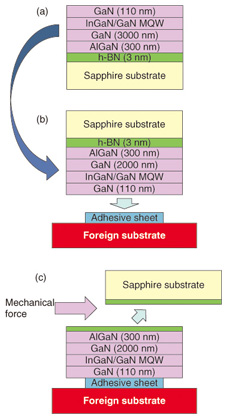
2. Experimental2.1 Growth processThe indium (In)GaN/GaN multiple-quantum-well (MQW) structure and the release and transfer processes are shown in Fig. 2. The h-BN release layer and the InGaN/GaN MQW structure were grown by MOVPE with hydrogen or nitrogen carrier gas. Triethylboron, trimethylgallium, trimethylaluminium, triethylgallium and trimethylindium were the group III source materials, and ammonia was the group V source. First, a single-crystal (0001) ultrathin h-BN layer with a thickness of 3 nm was grown on a (0001) sapphire substrate [9], [10]. The orientation relationship between the substrate and the h-BN was (0001)h-BN || (0001)sapphire. This indicates that the plane of boron and nitrogen was parallel to the substrate surface. Then, the InGaN/GaN MQW structure was grown on the h-BN release layer (Fig. 2(a)). The single-crystal h-BN layer works as the release layer. A flat single-crystal GaN layer can be grown on a single-crystal AlGaN or AlN layer on the h-BN despite the large lattice mismatch and the structural difference between the graphite-like (h-BN) shown in Fig. 1(a) and wurtzite (AlGaN and AlN) shown in Fig. 1(c).
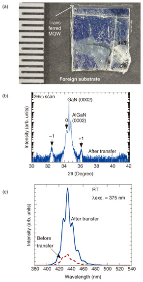
2.2 Transfer to foreign substrateAfter the growth, we flipped the MQW structure upside down and put it on a foreign substrate via an adhesive sheet (Fig. 2(b)). In this case we used an indium sheet as the adhesive; adhesive tape or glue would also work. Next, we heated the structure to a temperature sufficient to heat-seal the indium to the sapphire and the MQW. Finally, the MQW structure was released from the host sapphire substrate by mechanical force and thereby transferred to the foreign substrate (Fig. 2(c)). We call this transfer method “MeTRe” (Mechanical Transfer using Release layer). 3. Results and discussion3.1 Mechanical release of MQW structureA micrograph of the transferred InGaN/GaN MQW structure, approximately 25 mm2, is shown in Fig. 3(a). The structure is positioned on the indium sheet attached to the foreign substrate, as illustrated in Fig. 2(c). We also successfully transferred an AlGaN/GaN heterostructure, approximately 4 cm2, on the indium sheets. The size of the transferred area can be controlled by adjusting the adhesive sheet size. Some protrusions from the indium sheet, which are at the upper side of the structure, are discernible, indicating that the InGaN/GaN MQW structure with a thickness of about 3.5 μm is mechanically released from the host sapphire substrate. The surface of the indium sheet is seen through the transparent InGaN/GaN MQW. No cracks were observed in the upper half of the MQW structure, which suggests that the mechanical release process results in minimal crack formation.
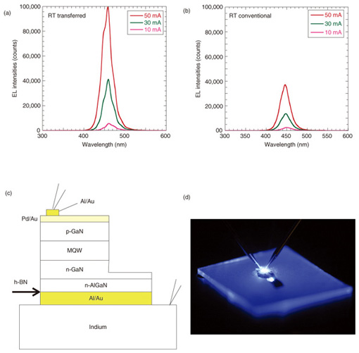
3.2 XRD resultsWe performed X-ray diffraction (using a 2θ/ω configuration) for the transferred MQW structure to check the crystal quality after the transfer. The X-ray diffraction (XRD) pattern in Fig. 3(b) shows satellite peaks from the MQW up to the first order, along with those for GaN (0002) and AlGaN (0002), without any trace of a sapphire (0006) peak. X-ray diffraction of the InGaN/GaN MQW structure before the transfer shows satellite peaks from the MQW, and peaks of GaN (0002), AlGaN (0002), and sapphire (0006). This means that the MQW structure consisting of the AlGaN layer, the GaN layer, the ten-period InGaN/GaN MQW structure, and the GaN cap layer, was successfully transferred, and the host sapphire substrate was mechanically released. It also supports the scenario that the separation occurs in the h-BN release layer, as shown in Fig. 2(c). The intensities of the satellite peaks up to the first order after the transfer are almost the same as those before the release, indicating that the MQW structure retains its original crystal quality. 3.3 XPS measurement resultsWe then performed X-ray photoelectron spectroscopy (XPS) measurements of the surfaces of the transferred film and the counter-surface of the sapphire substrate after the mechanical release to verify that the separation occurred in the h-BN. The B signal was obtained for both surfaces; the position of the B 1-s XPS peak for the transferred surface was the same as that for the counter-surface of the sapphire substrate, which indicates that the separation of the film actually took place at the h-BN release layer. 3.4 PL measurement resultsTo check the optical properties of the InGaN/GaN MQW after the transfer, we carried out room-temperature photoluminescence (PL) measurements on the MQW before and after the transfer. An InGaN-based semiconductor laser diode with an emission wavelength of 375 nm was used as the excitation source. The PL spectra from the MQW before and after the transfer are shown in Fig. 3(c). Both spectra show strong luminescence at almost the same peak wavelength of 434 nm. However, the intensity after the transfer is stronger than that before it because the indium sheet has high reflectivity in the visible wavelength region. We can also observe fringes in the PL spectrum after the transfer, suggesting that the surface of the transferred film is considerably flat. Indeed, atomic force microscopy images of the surface of the transferred films indicate that the surface is flat and has a root mean square roughness of 0.95 nm, which is consistent with the fringes in the PL spectrum in Fig. 3(c). 3.5 EL resultsNext, we describe the electroluminescence (EL) emitted from the transferred LED at room temperature. For comparison, we grew the LED structures on a typical LT-AlN buffer layer on a c-plane sapphire substrate and fabricated a conventional MQW LED without using a lift-off process. The LED structures consisted of a Si-doped AlGaN layer, Si-doped GaN layer, InGaN/GaN MQW structure, and Mg-doped GaN layer. The electron and hole concentrations in the Si-doped and Mg-doped GaN layers were 2 × 10¹⁸ and 3 × 1017cm-3, respectively. The EL spectra of the transferred LED and conventional LED for currents of 10, 30, and 50 mA are shown in Figs. 4(a) and (b). The EL intensities of the transferred MQW LED are comparable to or higher than those of the conventional LED grown on the LT-AlN buffer layer because of reflection from the back-side contact indium. Full width at half-maximum (FWHM) values of the EL of the conventional and transferred LEDs are almost the same for each current level. The comparable EL intensities and nearly the same FWHM values in Figs. 4(a) and (b) indicate that the MQW retained its original quality after the transfer. We also fabricated a vertical-type transferred LED (Fig. 4(c)), which can be achieved only when the LED is released from the host substrate. After the LED structure had been released, we deposited Al/Au electrodes on the back side of the LED and mounted it onto the indium sheet. An optical image of the EL from the vertical-type LED is shown in Fig. 4(d). We can clearly observe blue light emission from the vertical-type LED at room temperature.
4. Prototype fabricationWe used this mechanical transfer technique to fabricate a battery-powered LED prototype, in which the released LED was sandwiched between two laminates. The LED prototype emits violet-blue EL at room temperature. In addition, we released an InGaN/GaN LED from a sapphire substrate and transferred it to a piece of commercially available adhesive tape using MeTRe [11]. The MeTRe method has several advantages compared with conventional techniques. First, this approach requires no additional equipment and no chemical etchant. Second, the process is simple and can be completed within several seconds because the process harnesses the van der Waals forces of the h-BN to release the host sapphire substrate. Finally, the separated surface after the release is essentially flat because the separation tales place in the h-BN release layer. Accordingly, MeTRe is promising for reducing the cost of the release and transfer process. 5. ConclusionWe developed the MeTRe process for releasing GaN-based device structures from the host sapphire substrate and transferring them to foreign substrates. The mechanical transfer has been successfully used for AlGaN/GaN and InGaN/GaN MQW structures ranging in area from 25 mm2 to 4 cm2. We demonstrated that the intensities and FWHM of the transferred LED are comparable to those of a conventional LED, which confirms that the original device qualities are preserved even after the transfer using the MeTRe method. The MeTRe process will open up avenues of fabricating novel devices such as very thin LEDs, transparent solar cells sensitive only to ultraviolet light, and highly functional hybrid CMOS devices. References
|
||||||||||||||||||||||||