|
|||||||
|
|
|||||||
       |
Feature Articles: Optical Node and Switch Technologies for Implementing Flexible and Economical Networks Vol. 12, No. 1, pp. 42–47, Jan. 2014. https://doi.org/10.53829/ntr201401fa7 WSS Module Technology for Advanced ROADMAbstractWavelength selective switches (WSSs) are the key to implementing advanced reconfigurable optical add/drop multiplexing (ROADM) with colorless- directionless-contentionless (CDC) functionality, but a complex module (subsystem) requires a skillful balance combining optical, mechanical, and control design technologies. This article discusses technical issues in implementing WSS from optical, mechanical, and control perspectives. Keywords: WSS, MEMS, LCOS
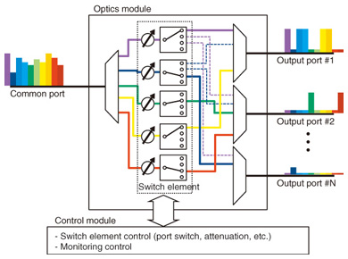
1. IntroductionWavelength selective switches (WSSs) are components used in wavelength division multiplexing (WDM) optical networks to route signals between optical fibers according to wavelength. The basic functions of WSSs are shown in Fig. 1. The main functions are switching by port switches, which are connected to output ports for each wavelength in the input WDM signal, and attenuation, in which the power level of transmitted light is adjusted for each wavelength. The hardware is divided into an optics module and a control module. A WSS has many input and output ports, so a bulk diffraction grating is used, which is able to multiplex and demultiplex signals at the same time in a single port. Active elements include a spatial light modulator device, for example, a microelectromechanical systems (MEMS) mirror [1], or a liquid crystal on silicon (LCOS) device, which can change the reflected direction of the input light beam. Beam pathways are different for each combination of wavelength and port, so beams cross each other within the WSS optical module. All of these pathways must be stable and have low losses, so the design of beam paths and spatial light modulator drivers and controls is very important in implementing appropriate attenuation. In addition to driving and controlling the switching element (spatial light modulator), the control module must detect module faults and errors, perform monitoring and control for coordination with higher-level systems, and provide a user interface.
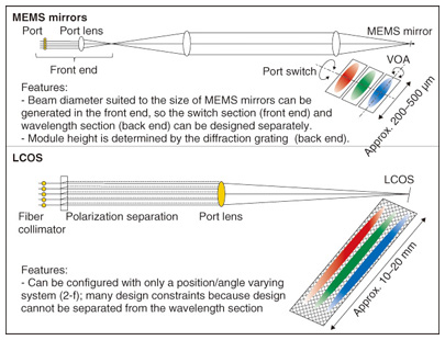
Technical issues in implementing WSSs are discussed below from the perspectives of optical, mechanical, and control (electronic monitoring and control) design. 2. WSS technical issues2.1 Optical designThe optical system for a WSS can be broadly divided into two sections: the wavelength section, which separates the input wavelengths using a diffraction grating, and the switch section, with its array of ports. The wavelength section design is basically a confocal optical system with the beam waists of the fiber end and MEMS mirror (or LCOS device) end. Wavelengths are separated spatially, so the configuration is similar to a high-resolution spectrometer. To achieve a wide transmission bandwidth, the beam diameter must be small at the MEMS mirror. However, this also reduces the depth of focus, so a meniscus lens or prism can be added for image correction. The switch section design differs depending on the type of switch element used. A comparison between MEMS mirrors and an LCOS device is shown in Fig. 2. With MEMS mirrors, it is more difficult to increase the size of the MEMS mirrors than to achieve a larger rotation angle, so the optical system for the switch section is divided into a front end and a back end. The front end generates a beam diameter that suits the size of the MEMS mirror. A confocal optical system, symmetric on either side of the diffraction grating, is generally used for the back end. For attenuation, optical axes are intentionally offset by rotating the MEMS mirror perpendicular to the switch face (wavelength face).
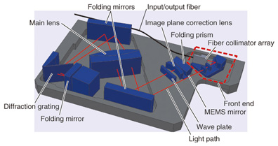
By contrast, with an LCOS device, instead of the advantage of providing a large reflection surface on the order of millimeters, the device generates diffraction losses (excessive losses) using a large diffraction angle. Thus, when an LCOS device is used, the switch section can be implemented with just a 2-f optical system* for the front end. This configuration may seem simple, but it is inseparable from the wavelength section, so there are many design constraints. LCOS devices are also polarization dependent, which presents other difficulties such as the need for a polarization diversity configuration. With these forms used as a base, an optimal design must satisfy WSS performance specifications (number of ports, bandwidth, losses, cross-talk, size, etc.), while considering switch element characteristics (rotation angle, size, losses, etc.). Lens and optical system aberrations are related to the dependence of losses and bandwidth on wavelength and port, and residual stray light causes degradation due to transmission ripple and cross-talk. Aberration and stray light are therefore significant problems. When the number of ports is increased in the future, there will be room to work with the arrangement of the ports, and configurations such as 2D port arrangements have been proposed. There are also other devices besides the MEMS mirrors and LCOS devices discussed above that can be used as switch elements, for example, digital micro-mirror devices and transmission-type LCDs (liquid crystal displays). LCOS and DMD devices are composed of small pixel elements, so they are suitable for FlexGrid applications. 2.2 Optical module designThe optical module is composed of optical components such as lenses and switch elements, as well as mechanical components for maintaining highly accurate positioning of the optical components. The shape and position of the optical components were determined through simulation in order to achieve the desired optical design characteristics. To implement these characteristics at the module level, the production variances and accuracy of alignment in assembly are verified and are taken into consideration while designing the configuration and assembly procedures. Also, in order to achieve the high wavelength accuracy and stable transmission characteristics needed for the WSS, a final process had to be planned. This process involved aligning the element positions and checking the characteristics while actually passing light through the system, and then fixing the positions. In theory, a WSS is a three-dimensional (3D) optical system that must be of sufficient size and that has light paths expanding in both the wavelength and switch axis directions. However, in actual devices, reflective mirrors are used to fold up the light paths and achieve a compact design configuration. Reducing the size of the optical system not only reduces the size and weight of the module, it is also important for increasing the mechanical strength, reducing dependencies on environmental factors, and maintaining stable optical characteristics. A schematic diagram of the 1 × 9 WSS optical module developed by NTT is shown in Fig. 3. A compact and stable module is implemented by arranging each optical element in 3D on an alloy block with a low thermal-expansion coefficient.
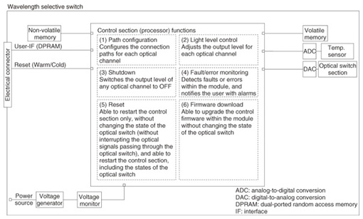
The WSS module is built as a hermetically sealed structure for two reasons. The first is that the refractive index of air is dependent on environmental factors such as air temperature and pressure, and this can cause fluctuations in the diffraction angles of the diffraction grating, and thus, in the WSS channel wavelengths. Creating a hermetically sealed structure fixes the air density and controls the channel wavelength fluctuation within the level needed for current high-density WDM systems. The second reason is that changes in internal humidity can reduce the reliability of MEMS mirrors or LCOS switch elements. By maintaining low internal humidity in the structure, the high stability and reliability required of a telecommunication device can be maintained, even when used in high-temperature environments. Also, when MEMS mirrors are used, the characteristics can fluctuate due to its structural resonances, and anti-vibration structures such as rubber dampers must be used to prevent damage. For the 1 × 9 WSS using MEMS mirrors, hermetically sealed conditions for the optical module were achieved by fixing it in a hermetic case with a rubber damper, fixing the cover to the hermetic case using welding techniques, and passing input/output fibers and MEMS driver electrical terminals through a solder seal. 2.3 Electrical monitoring and controlElectrical monitoring and control drives and controls the active elements of the optical module (the spatial light modulator), and also detects any faults or errors in the module, provides the monitoring and control required for linking with higher-level systems, and controls the user interface. The overall control structure of the WSS module is shown in Fig. 4. This module is composed of a control process, a voltage generator/monitor section, volatile and nonvolatile memory, temperature sensors, and other components, which are used to control the optical module described above (optical switch in the diagram). The control processor performs control processing for the switch device in the optical module (MEMS mirror or LCOS device) and also processes control signals such as resets or commands sent by the user, monitors for faults or errors in the WSS module, and notifies the user if any such fault or error occurs in the module. Communication with the user (commands, reset, alarms, etc.) occurs through the electrical connectors.
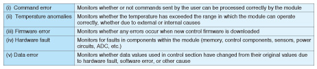
Control in the WSS module is divided into six functions: (1) Path configuration, (2) Light level control, (3) Shutdown, (4) Fault/error detection, (5) Reset, and (6) Firmware download (Fig. 4). Implementing monitoring functions as a subsystem of the WSS module is important, and the fault/error monitoring functions are described in detail below. The WSS control module monitors fault/error items including: command errors, temperature anomalies, firmware errors, hardware faults, and data errors (Table 1).
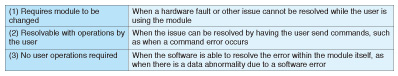
If a fault or error occurs while the WSS module is operating, the effects on the user are categorized into one of three levels (Table 2).
- The module must be changed - The issue can be resolved through user operations - The issue does not require user intervention Thus, when a fault or error occurs, it is important to consider the effect of the problem on the user as described here when determining what sort of alarm or notification will be sent to the user.
3. Future prospectsAs discussed above, the WSS module was implemented by combining a wide range of technologies. For example, even for the thermal characteristics alone, it was necessary to coordinate a wide range of design techniques. These included optical design to consider how the refractive index of glass depends on temperature, mechanical design to consider the thermal deformation of parts and the effects of environmental changes, and control design to compensate for temperature issues. In the future, it will be necessary to further increase the bandwidth and number of ports for the WSS, and a much greater level of coordination will be necessary. Regarding the FlexGrid, a WSS using an LCOS device has been progressing, but while it is possible to control an LCOS device at the pixel level, driver control at that level is very complex. Manufacturing that is able to skillfully coordinate optical, mechanical, and control design techniques is expected to drive the development of ROADM with CDC functionality. Reference
|
||||||