|
|||||||||||||
|
|
|||||||||||||
       |
Feature Articles: Optical Node and Switch Technologies for Implementing Flexible and Economical Networks Vol. 12, No. 1, pp. 48–52, Jan. 2014. https://doi.org/10.53829/ntr201401fa8 Multicast Switch Technology that Enhances ROADM OperabilityAbstractA multicast switch is a compact and cost-effective optical switch that realizes a colorless, directionless, and contentionless function and enhances the operability of a multi-degree reconfigurable optical add/drop multiplexer. This article describes the circuit configuration and characteristics of the multicast switch, which employs a silica-based planar lightwave circuit. Keywords: ROADM, optical switch, PLC
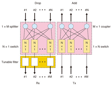
1. Overview of CDC functionA colorless, directionless, and contentionless (CDC) function enables us to connect optical add/drop signals at any wavelength and from/to any direction in a multi-degree reconfigurable optical add/drop multiplexer (ROADM) to local transponders without any signal contention. ROADM systems are advantageous in that wavelength division multiplexing (WDM) optical signals can be routed individually without optical-electrical conversion, and they have been evolving from ring to multi-degree ROADM systems. A multi-degree ROADM can select wavelength-by-wavelength whether an incoming WDM signal from any direction will pass through the node and continue in any direction or will be added/dropped at the local node. However, in a conventional ROADM, the wavelength and direction of the optical add/drop signals are assigned in terms of the port to which they are connected, and this makes it necessary to reconnect optical fibers to transponders manually. A multi-degree ROADM with a CDC function that makes it possible to connect optical signals with any wavelength in any direction to any transponder enhances system operability and enables us to construct more flexible and reliable networks. 2. TPA using multicast switchTo realize the CDC function, an optical switch that can assign any wavelength and any direction to each transponder must be employed between the add/drop ports and the transponders. This switch is called a transponder aggregator (TPA). An N × M TPA is required on both the drop and add sides; here, N is the number of input/output routes, and M is the number of transponders. In the TPA, WDM signals are incoming from or outgoing to the ROADM, while a single wavelength is received from or sent to the transponders. On the drop side, the capability to connect different wavelength signals from the same direction to different transponders is required, while on the add side, the capability to launch different wavelength signals from different transponders in the same direction is required. Among TPA configurations, the multicast switch offers a compact and cost-effective TPA. The TPA architecture that employs a multicast switch is shown in Fig. 1. In a multicast switch on the drop side, WDM signals from each direction are broadcast by a 1 × M splitter, and the signals from the desired incoming fiber are selected by an N × 1 optical switch. A WDM signal at the desired wavelength is extracted by a tunable filter, and then the selected signal is received by the transponder. This architecture enables us to select an optical signal at any wavelength from any direction. The same wavelength signals from other input directions are rejected by the optical switch, which eliminates any signal contention in the TPA.
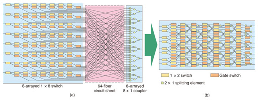
On the add side, the output signals from the transponders are routed to a desired outgoing fiber by a 1 × N switch array, combined with different wavelengths by an M × 1 coupler, and then launched into the add ports of the ROADM. This architecture enables us to send an optical signal at any wavelength in any output direction. The advantage of a TPA using a multicast switch is that it is composed of compact optical components including optical splitters and switches. This is unlike a TPA, which uses a wavelength selective switch (WSS) or a large matrix switch. Although a multicast switch has an intrinsic splitting loss because it includes an optical splitter, we can compensate for this loss with an optical amplifier. A multicast switch based TPA also has the advantage that its switch scale can be expanded by cascading optical splitters when the number of transponders increases. Thus, it is suitable for multi-degree ROADMs that have a small number of add/drop signals. 3. Multicast switch using PLC3.1 Circuit configurationAn optical switch using a silica-based planar lightwave circuit (PLC) is operated by the thermo-optic effect of silica-on-silicon waveguides. It offers good reliability and mass producibility because it has no moving parts, and many chips can be fabricated simultaneously in wafer processing [1]. Another advantage is that many functional elements can be integrated, thus making it suitable for constructing a multicast switch. As shown in Fig. 1, the TPAs on both the drop and add sides comprise N units of 1 × M splitters (or M × 1 couplers) and M units of 1 × N switches that are interconnected, and they are identical except for the tunable filters on the drop side. This architecture is the same as that of an optical switch used for photonic transport systems [2], and an 8 × 8 switch was fabricated using a PLC. However, the conventional switch comprises 8-arrayed 1 × 8 switches and 8-arrayed 8 × 1 couplers, and those chips are separated and connected via a 64-fiber circuit sheet as shown in Fig. 2(a) to avoid having too many waveguide crossings on a PLC chip. They were packaged into a 240 mm × 95 mm × 12.5 mm module [3]. We recently developed a new circuit configuration that integrates the splitter and switch [4], as shown in Fig. 2(b). The 8-arrayed 1 × 8 switch comprises eight 1 × 2 switch elements cascaded serially, with a gate switch placed after each 1 × 2 switch element. We divided the 8 × 1 coupler into 2 × 1 elements, and placed them between the stages of the switch elements. This new circuit configuration reduces the maximum number of waveguide crossings by three fourths, and establishes an even number of them between the paths. This allows single chip integration of the 8 × 8 multicast switch and makes it possible to eliminate the fiber circuit sheet, which reduces the size of the optical switch module as described below.
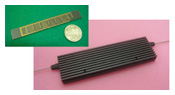
3.2 Fabricated PLCWe fabricated an 8 × 8 multicast switch using a PLC based on the architecture shown in Fig. 2(b). The 1 × 2 and gate switch elements are based on a Mach-Zehnder interferometer with a path difference of half a wavelength between its arms. When we activate a thermo-optic phase shifter, optical outputs between the two ports are switched in 2 ms [1]. The fabricated chip and module are shown in Fig. 3. The chip is 110 mm × 15 mm, and the fiber pig-tailed module is 150 mm × 45 mm × 13 mm, which is one third the size of the conventional module.
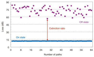
3.3 Optical performanceThe measured performance of the multicast switch is shown in Fig. 4. The average insertion loss of the switch was 11.9 dB with a maximum value of 12.0 dB. This is the same as that of a conventional switch using a fiber circuit sheet. The loss includes an intrinsic splitting loss of 9 dB and an excess loss of 3 dB. The waveguide crossing induced loss was estimated to be 1 dB. The average and maximum polarization dependent losses (PDL) were 0.13 and 0.22 dB, respectively. The average wavelength dependent loss (WDL) between 1530 and 1570 nm was 0.66 dB, and the maximum value was 1.10 dB. The average and minimum off-state losses were 62.6 and 42.4 dB, respectively. We employed heat-insulating grooves to reduce power consumption. The average electrical switching power was 0.2 W per path, and the total power consumption was 1.6 W. This performance is satisfactory for practical applications.
We also fabricated an 8 × 12 multicast switch based on the circuit configuration [5]. The average and maximum insertion losses of the 8 × 12 multicast switches were 14.1 and 14.5 dB, respectively, including an intrinsic splitting loss of 10.8 dB. The PDL was less than 0.2 dB. The average WDL between 1530 and 1570 nm was only 0.1 dB, and the maximum value was 0.3 dB. The average extinction ratio between the on and off states was 59.2 dB, and the minimum value was 45.4 dB. These results indicate the good scalability of the PLC-based multicast switch. 4. ConclusionWe described the circuit configuration and the performance of an N × M multicast switch that integrates 1 × M splitters and 1 × N switches into a single PLC chip. This PLC-based multicast switch enables us to realize a multi-degree ROADM with a CDC function cost effectively and with a small footprint. We plan to reduce the power consumption further and enhance the optical performance of the PLC-based multicast switch. References
|
||||||||||||