|
|||||||||||||||||||||||||||||||||||||||||||||||||||||||||||||||||||||||
|
|
|||||||||||||||||||||||||||||||||||||||||||||||||||||||||||||||||||||||
       |
Regular Articles Vol. 12, No. 8, pp. 30–36, Aug. 2014. https://doi.org/10.53829/ntr201408ra1 High-temperature Superconductivity without Doping—Synthesis of Conceptually New SuperconductorsAbstractHigh-temperature superconductivity is commonly associated with cuprate superconductors as their superconducting transition temperatures are still highest among all of the superconducting materials. It is these cuprate superconductors that drive scientists to reveal the very mechanism of its superconductivity and to derive models capable of predicting new superconducting material systems. Cuprate superconductors are built up of copper-oxygen planes, sandwiched by rare-earth or alkaline-earth oxide layers. The copper-oxygen layers form infinitely long planes, and it is those planes where superconductivity takes place. In particular, the copper ions in those planes may have three distinct coordinations, i.e., octahedral, pyramidal, and square-planar. Quite generally, electronic states are a function of crystal structure, crystal symmetry, and the elements building up the crystal structures. Nevertheless, it has been widely assumed that the copper-oxygen planes are inherently insulating and superconductivity is induced by doping carriers into those copper-oxygen planes. Indeed, such an approach is suitable for the copper-oxygen layers with octahedral and pyramidal coordinated copper, where superconductivity is induced by hole doping. For cuprates with square-planar coordinated copper, however, we demonstrate here that elimination of defects by annealing is the key to inducing superconductivity and doping is not a prerequisite for the emergence of superconductivity. Keywords: undoped superconductor, high-Tc cuprates, molecular beam epitaxy
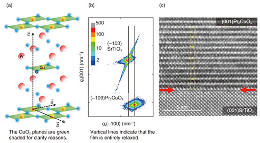
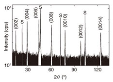
1. IntroductionHigh-temperature superconductivity is a key technology for many present and future milestones ranging from transportation [1], over medical applications [2] towards elementary particle physics [3]. Among all superconducting materials known so far, the discovery of cuprate superconductors was not only awarded by the Nobel prize [4] but still hold record high superconducting transition temperatures as high as 150 K [5]. Despite all efforts and progress made to understand the underlying mechanism driving superconductivity in those cuprates, conclusive theoretical models remain elusive. Solving the enigma of cuprate superconductivity, however, holds the key for materials with even higher superconducting transition temperatures. One of the crucial factors that drives superconductivity in cuprates are the copper-oxygen planes and the local environment of the Cu ions in those planes. Generally, three different geometries are stabilized in cuprate superconductors, i.e., octahedral, pyramidal, and square-planar. In many cases, those coordination cages do not appear exclusive but as combinations, e.g., pyramidal and square-planar in Bi2Sr2Ca2Cu3O10+δ. The local coordination of the copper ions has far reaching implications on the electronic structure. Revealing electronic structures subject to a specific coordination is therefore of importance. La2-xSrxCuO4 is a cuprate with solely octahedrally coordinated copper and it is one of the most widely studied systems among cuprate superconductors and commonly termed “T-phase.” Cuprates with solely square-planar coordinated copper are much less studied owing to the difficult and cumbersome process in synthesis as well as inducing superconductivity to them. Hence, data reported for these systems are significantly dressed and dominated by electronic correlations stemming from impurity and defect related influences. In contrast to those earlier reports, we can synthesize cuprate superconductors by molecular beam epitaxy under oxidizing conditions. Molecular beam epitaxy is a well-known and widely used technique for synthesizing semiconductors and semiconductor-related devices. We further refined and optimized this technique with the scope of ultra-high quality cuprate materials [6]. Crystalline materials with the utmost degree of perfection are mandatory prerequisites in revealing electronic and magnetic correlations in cuprates with respect to the various coordination geometries of copper. Two cuprates, where copper is square-planar coordinated, are known, i.e., Nd2CuO4–structure [7, 8] and infinite-layer structure [9]. While the Nd2CuO4–structure (T’-structure) can be synthesized under ambient conditions, the formation of bulk infinite-layer cuprates occurs only under high pressure. The T’-structure belongs to the Ruddelsden-Popper series of transition metal oxides [10–12], which is also the case for the T-structure. In contrast to other transition metal oxides, where the transition metal ion is octahedrally coordinated, the copper ion is forced to be square-planar coordinated in the T’-structure and the force is brought by the tolerance factor [13]. The defects appear at the apical position of copper, forming locally pyramidal coordinated copper. Electronically, this situation represents an insulating and antiferromagnetic ground state. Upon elimination of those defects (by elaborate annealing), the entire electronic structure changes from an antiferromagnetic insulator to a superconducting metal. In the following we focus on our efforts to elucidate the electronic structure of ultra-high quality T’-cuprate superconductors where such defects have been eliminated by annealing. 2. ExperimentalHigh quality thin films of Pr2CuO4 are grown by molecular beam epitaxy onto (001) SrTiO3 substrates [14]. Pr and Cu are evaporated by e-beam evaporation from metal-sources and the evaporation rate is controlled by electron impact emission spectroscopy [15–18]. Ozone or radio frequency (RF) activated oxygen is used as an oxidizing agent. The growth is monitored by reflection high energy electron diffraction (RHEED) which allows not only fine tuning of growth conditions but a real-time feedback of film growth. In Fig. 1, the crystal structure of Pr2CuO4, high-resolution reciprocal space map (HRRSM) of the epitaxial relation, and high-resolution transmission electron microscopy (HRTEM) image of Pr2CuO4 films on (001) SrTiO3 substrates are shown, respectively. Here, growth conditions are tuned in order to allow for a relaxed but epitaxial growth of single phase and c-axis oriented Pr2CuO4 on SrTiO3. Throughout the following experiments and discussions, the film thickness was kept constant at 100 nm. In Fig. 2, X-ray diffraction of a Pr2CuO4 film on (001) SrTiO3 substrate is shown. Using a Nelson-Riley [19] function allows for a precise determination of c-axis lengths as this is an important control parameter.
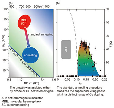
As discussed in the introduction, the as-grown Pr2CuO4 is insulating due to the presence of over-stoichiometric oxygen occupying the apical sites of copper [20–24]. As it is well known from Ce doped Pr2-xCexCuO4, annealing is required for the induction of superconductivity—otherwise, the system remains insulating and antiferromagnetic. During the annealing process, the apical oxygen leaves the Pr2CuO4 crystal. Such a process is a diffusion process though in case of Pr2CuO4 a detailed understanding remains elusive owing to the three different oxygen positions in the T’-crystal structure [25–29]. Here, we applied a two-step annealing process [15], which allows for an effective evacuation of apical sites, while regular oxygen positions are not affected. The annealing procedure requires that thermodynamic constraints of Pr2CuO4 itself are not violated (this leads to decomposition). At the same time, an appropriate annealing is achieved only near or on thermodynamic boundary on a delicate balance of kinetically driven competition. 3. Results and discussions3.1 Standard annealingThe term “standard annealing” may seem confusing though it simply describes annealing conditions used for the induction of superconductivity at doping levels of x = 0.15; i.e., Pr1.85Ce0.15CuO4 [30, 31]. As annealing of Ce doped Pr2CuO4 is carried out under ultra-high vacuum, only two annealing parameters, time and temperature, are to be considered. Applying the standard annealing approach leads to phase diagram of Pr2-xCexCuO4 as shown in Fig. 3. At low Ce doping levels (x < 0.11) the system is insulating and superconductivity sets in for x > 0.12. This phase diagram (Fig. 3) inevitably is identical to what has been reported for single crystals or powder samples.
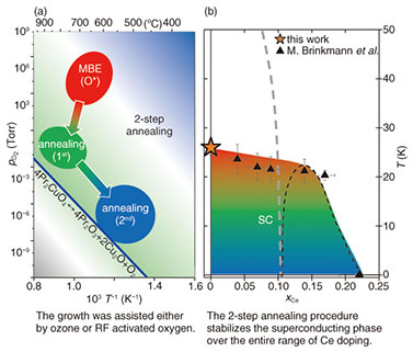
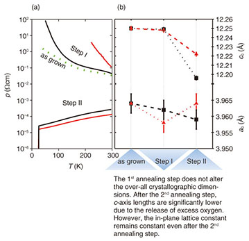
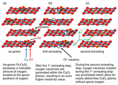
3.2 2-step annealingApplying standard annealing conditions to Pr2-xCexCuO4 is effective for the induction of superconductivity for x > 0.11. In Pr2-xCexCuO4, the addition of Ce not only acts as a dopant but as a defect [32]. If less Ce is incorporated into the Pr2-xCexCuO4 crystal, the crystallite dimensions rapidly increase. The path taken by oxygen leaving Pr2-xCexCuO4 crystals is predominantly along the CuO2 planes until reaching a grain boundary. The thermodynamic environment under standard annealing conditions is unsuitable for establishing such a condition over long periods of time or at elevated temperatures due to the simultaneously occuring defects at regular oxygen sites. This diffusion problem of identical species at competing sites is not limited to thin film but to a much larger extent to single crystals owing to their reduced surface/volume ratio. However, this problem can be overcome by introducing an intermediate annealing step. This situation is visualized in the thermodynamic phase diagram plotted in Fig. 4. In contrast to the standard annealing procedure, Pr2CuO4 is kept at a temperature comparable or even higher than the synthesis temperature used during its growth [33]. Moreover, an environment with small but finite partial oxygen pressure is stabilized for 60 min before the sample temperature is cooled to the second annealing step. In Fig. 5, the temperature dependence of resistivity is plotted for all three positions of the thermodynamic phase diagram. The as-grown Pr2CuO4 is insulating and its resistivity further increases after the 1st annealing step. This behavior indicates that additional defects, tapering the electron mobility, are created. Schematically, this is shown in Fig. 6. While the as-grown Pr2CuO4 posseses defects primarily related to occupied apical sites, the first annealing step is about to increase the defects within the CuO2 planes. Consequently, the absolute resistivity value increases. Simultaneously, the overall crystallographic dimensions remain nearly unaffected. This does change, however, dramatically after the second annealing step and the c-axis value shrinks noticably. Most dramatic is the influence on the resistivity behavior as it not only changes from an insulating to a metallic state but to superconductivity. This behavior is again common to what is known to happen during the conventional annealing process for Ce-doped Pr2-xCexCuO4 (x > 0.11). Accordingly, our study has revealed an intrinsic electronic phase diagram for Pr2-xCexCuO4, which was hampered by enigmatic and cumbersome processes in optimizing annealing conditions.
4. ConclusionIt has been assumed that the high-Tc cuprates universally have an insulating ground state in their undoped state due to electronic correlations, and doping is necessary to change the correlations and induce superconductivity. However, a series of our studies have revealed that the cuprates with the square-planar coordinated Cu have a metallic ground state and show superconducting transition after removal of defects from the playground of high-Tc superconductivity, i.e., the copper-oxygen planes. This observation is against the main paradigm in theories of high-Tc superconductivity. Although, at the moment, this conclusion is still under intense debate, the very result of our research will be a turning point in the quest for high-Tc superconductivity once further investigations support it. References
|
||||||||||||||||||||||||||||||||||||||||||||||||||||||||||||||||||||||