|
|||||
|
|
|||||
       |
Practical Field Information about Telecommunication Technologies Vol. 13, No. 6, pp. 32–36, June 2015. https://doi.org/10.53829/ntr201506pf1 Method to Identify Conducted Disturbance Source of Malfunction of Telecommunication ServicesAbstractThis article introduces equipment used to identify a conducted disturbance source in telecommunication equipment. This is the twenty-ninth of a bimonthly series on the theme of practical field information on telecommunication technologies. This month’s contribution is from the EMC Engineering Group, Technical Assistance and Support Center, Maintenance and Service Operations Department, Network Business Headquarters, NTT EAST. Keywords: conducted disturbance, noise direction detector, malfunction in telecommunication equipment
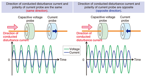
1. IntroductionMany kinds of devices such as telephones, personal computers (PCs), and televisions incorporate communication functions. These devices are connected to the Internet through a home gateway. In this environment, a conducted disturbance that is generated by a fault in one device can lead to malfunctions in other devices such as audible noise in a telephone or a communication error in a PC. When a malfunction occurs, the conducted disturbance source (i.e., the device with the fault) needs to be identified and then repaired or removed. However, in a communication environment in which multiple communication devices and home appliances are connected to the same mains and telecommunication network, identifying the conducted disturbance source can be extremely difficult. If the source cannot be identified, it becomes necessary to reduce the conducted disturbance by inserting a noise filter, for instance, a common-mode choke coil, on the telecommunication line (telephone line, Ethernet cable, etc.) and/or the mains line of the malfunctioning telecommunication devices affected by the conducted disturbance. However, a countermeasure based on the insertion of a noise suppression filter incurs a cost and might have to be applied to another connected device if it is later found to be affected by a conducted disturbance. Accordingly, identifying the conducted disturbance source and repairing or removing the source is a more effective countermeasure than inserting noise filters. Therefore, the EMC Engineering Group has proposed a simple and efficient method for identifying a conducted disturbance source and has constructed a prototype device for identifying the direction of conducted disturbance propagation. This article describes this simple method for identifying the conducted disturbance source and explains the effectiveness of the prototype device. 2. BackgroundWhen responding to a malfunction in telecommunication equipment caused by a conducted disturbance, maintenance personnel use the following procedure to identify the conducted disturbance source in the field. (1) Measurement of conducted disturbance: Measure the conducted disturbance voltage and frequency at the telecommunication or mains port of the telecommunication equipment affected by the conducted disturbance. (A noise search tester can be easily used for measuring the voltage and frequency.) (2) Relationship between conducted disturbance and malfunction: Confirm that the malfunction occurs synchronously with the conducted disturbance. (3) Check the flow of the conducted disturbance current: Compare the conducted disturbance voltage levels at telecommunication and mains ports. Estimate the conducted disturbance current from the comparison results. (4) Identify the conducted disturbance source: Find the conducted disturbance source with the highest voltage level and repair or replace it. The conducted disturbance source can generally be identified by following the above procedure. However, when a malfunction is caused by a fault in the power supply section of a device, and multiple devices are connected to the same mains line via a multi-plug, the same conducted disturbance voltage level would be measured at all of the mains ports of each device. To identify the conducted disturbance source in this case, we need to turn off the power supplies of all connected devices. However, it is not usually possible to turn off the power supplies of all devices. There is therefore a need for a device that can identify a conducted disturbance source and the direction of its propagation even when conducted disturbance voltage levels are identical. 3. Identifying conducted disturbance source3.1 PrincipleConducted disturbance voltage measurement can only be applied to check the level of conducted disturbance voltage, which may be ineffective for identifying the conducted disturbance source, as described previously. Therefore, we focus on the direction of conducted disturbance current. However, measuring only the conducted disturbance current does not establish which direction the current is flowing. To resolve this problem, we have developed a method for identifying the direction of conducted disturbance propagation by simultaneously measuring conducted disturbance voltage and current [1]. A diagram of the proposed method is shown in Fig. 1. A capacitive voltage probe and current probe are used to measure the conducted disturbance voltage and current.
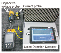
As shown in Fig. 1, the current probe has polarity. If this polarity points in the same direction as the flow of conducted disturbance current, the voltage and current will be in phase (the time waveforms of voltage and current are superposed), but if it points in the opposite direction, the voltage and current will be out of phase (the time waveforms of voltage and current are offset). This feature can be used to identify the direction of conducted disturbance propagation. 3.2 PrototypeAn external view of the device used to identify the direction of conducted disturbance propagation that we developed is shown in Fig. 2. We call this device a Noise Direction Detector (NDD). The NDD has capacitive voltage and current probes for measuring conducted disturbance voltage and current, a signal processing section that inputs measured conducted disturbance current and voltage, and a display section for presenting the results of calculating the conducted disturbance propagation direction. The display section is a tablet terminal with a touch screen.
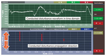
The display section is shown in Fig. 3. If conducted disturbance current is flowing in the same direction as the orientation of the current probe, the measured values will be displayed in the positive direction on the graph. If current is flowing in the opposite direction, the values will be displayed in the negative direction. The results shown in Fig. 3 are those for a conducted disturbance current flowing in the same direction as the orientation of the current probe.
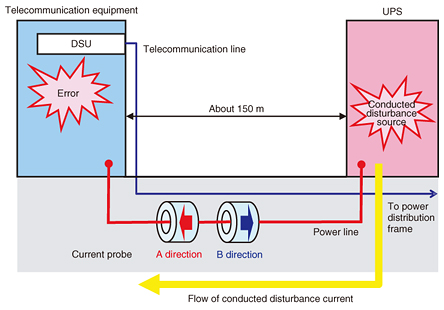
4. Evaluation of NDDWe present a case study in which the NDD was applied and the conducted disturbance source was identified for a telecommunication malfunction that occurred inside a telecommunication building. 4.1 Malfunction overview and facility layoutA customer claimed to be experiencing telecommunication errors on a digital circuit that made the customer’s system unusable. Maintenance personnel checked the telecommunication conditions and confirmed that telecommunication errors were occurring. The customer’s facility layout is shown in Fig. 4. In this layout, the digital service unit (DSU) has telecommunication and mains ports. The mains port of the DSU is connected to an uninterruptible power supply (UPS) in the power room via a power distribution frame.
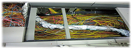
4.2 Measurement of conducted disturbanceIt was necessary to verify that the communication errors that were occurring were due to conducted disturbance. The conducted disturbance voltage was measured in both the telecommunication and mains ports of the DSU. The measurement results revealed conducted disturbance voltage with a peak at about 200 kHz superposed on the transmission band of the digital circuit. In addition, the conducted disturbance voltage level at the mains port of the DSU was higher than that of the telecommunication port, so it was inferred that the conducted disturbance was propagating via the mains port of the DSU. 4.3 Identification of conducted disturbance sourceConducted disturbance measurements therefore confirmed that the conducted disturbance was propagating from the mains port of the DSU. However, many power supply lines and communication lines are laid under double floors in telecommunications buildings, as shown in Fig. 5, and furthermore, many units of communication equipment are connected via a power distribution frame.
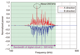
Consequently, when the conducted disturbance voltage of power supply lines connected to the power distribution frame was measured, nearly the same level of conducted disturbance voltage was observed on all power supply lines that were measured. The NDD was therefore applied to this power distribution frame to determine the conducted disturbance propagation path. The orientations of current probes are shown in Fig. 6, and the measurement results are shown in Fig. 7. These results revealed that the conducted disturbance was propagating from the upper side (power room side) of the power supply line. Then, the same kinds of measurements were repeated, and the source of the conducted disturbance was soon found to be the UPS unit installed in the power room. The UPS manufacturer was consulted, and it was found that a UPS component had failed. The UPS unit was replaced, which eliminated the malfunction in the DSU.
5. ConclusionWe reported on the development of a device used for identifying the direction of conducted disturbance propagation and confirmed that the device was effective in identifying an actual communication malfunction that occurred inside a telecommunication building. We plan to develop a more compact version of this equipment for use in field operations. Malfunctions in telecommunication equipment due to conducted disturbance can occur in all types of places including telecommunication buildings, inside homes, and even outdoors. Looking forward, the EMC Engineering Group of the Technical Assistance and Support Center is committed to participating in technology dissemination activities such as technology collaboration, technology development, and technology seminars to contribute to the prompt resolution of malfunctions in telecommunication equipment and the smooth provision of telecommunication services. Reference
|
||||