|
|||||||||||||||||||
|
|
|||||||||||||||||||
       |
Feature Articles: Frontier Research on Low-dimensional Semiconductor Physics Vol. 13, No. 8, pp. 5–10, Aug. 2015. https://doi.org/10.53829/ntr201508fa2 High-speed Single-electron Transfer toward High-accuracy Current StandardsAbstractSingle-electron transfer is a technique for manipulating single electrons to generate an accurate electric current, which is expected to be used as a new current standard. Realization of the current standard is important for performing quantum metrology triangle experiments, with which we can confirm the accuracy of fundamental physical constants, and it could be a contributing factor in redefining the ampere. NTT Basic Research Laboratories has been studying single-electron transfer using silicon transistors. In this article, we discuss high-speed single-electron transfer via a small island electrically formed using silicon transistors and via a trap level in silicon. Keywords: single-electron transfer, silicon transistor, current standard
1. Single-electron transfer and current standardsSingle-electron (SE) transfer is a technique for conveying electrons one by one in synchronization with a clock signal. It has been extensively studied using solid devices mainly fabricated from metals or semiconductors. An accurate current flow generated by SE transfer is expected to be used as a new current standard, which corresponds to a measure of electric current. Realization of the current standard could lead to the redefinition of the ampere (Fig. 1(a)), which has recently attracted much attention. The definition of the ampere is presently referenced to a force produced by the same current flowing through two infinite-length conductors in a vacuum, and it is therefore difficult to achieve the exact conditions described in the definition in actual experiments. In a practical sense, the definition has the effect of fixing the value of the vacuum permeability (with a unit of m·kg·s−2·A−2). In addition, because the ampere depends on the units of length, mass, and time, the accuracy of the ampere is strongly affected by the change in the weight of the international prototype kilogram*1, which is the only artifact among the standards and defines mass. To eliminate such uncertainty originating from the artifact, the abolition of the international prototype kilogram was proposed in 2011 (and will be carried out after 2018), and, along with the abolition, the ampere will also be redefined. In the redefinition, the ampere is set by fixing the numerical value of the elementary charge e. SE transfer can generate accurate current with a value of e × f simply using an input clock signal with frequency f, which can be obtained with the highest accuracy among all standards. It is therefore expected to be used as an ultimate current standard that enables the ampere to be directly set with a single device. In addition, an important milestone for achieving the new current standard is the quantum metrology triangle experiment (Fig. 1(b)). In this experiment, the current generated from a current standard using SE transfer is compared with that generated from a combination of the quantum Hall resistance standard*2 and the Josephson voltage standard*3, which are now used in the International System of Units (SI). If SE transfer with sufficiently high accuracy can be achieved, the accuracy of the von Klitzing constant RK = h/e2, where h is the Planck constant, and the Josephson constant KJ = 2e/h would be verifiable through the experiment, which could lead to the realization of more accurate electrical standards.
For application to the current standard, the device should be able to generate a wide range of current. However, because e is a tiny value (~1.6 × 10⁻¹⁹ C), many electrons must be carried to obtain a large current level. For example, high-speed SE transfer with a gigahertz transfer frequency is necessary to perform the quantum metrology triangle experiments with high accuracy. In addition, since the accuracy of the present electrical standards is about 10−8, the accuracy of SE transfer should be below 10−8. SE transfer has so far been studied using various systems, but devices that can simultaneously satisfy both the speed and accuracy requirements have not yet been developed. At NTT Basic Research Laboratories, we have been studying SE transfer using silicon devices as part of efforts to achieve high-speed and high-accuracy SE transfer. With silicon, we should be able to stably fabricate devices that can be used for the current standard because we can use well-established device fabrication techniques accumulated through developments in the semiconductor industry. In this article, we introduce tunable-barrier SE transfer devices, which can be operated at high speed.
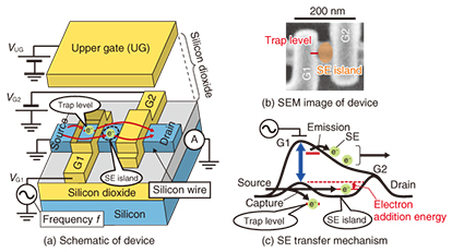
2. Silicon tunable-barrier SE transfer devices: transfer via an SE islandA schematic and an SEM (scanning electron microscope) image of the silicon tunable-barrier SE transfer device are respectively shown in Figs. 2(a) and 2(b). We used electron beam lithography to fabricate silicon transistors that have double-layer n+-doped polycrystalline-silicon gate electrodes on a silicon wire with a width of a few dozen nanometers. Each lower gate (G1, G2) induces a potential barrier in the silicon wire, leading to the formation of a small region between G1 and G2 (hereafter called an SE island) in which electrons are confined. The upper gate (UG) is used to modulate the electron potential in the SE island. To perform SE transfer via the SE island, we apply high-frequency signal VG1 with frequency f to G1, with fixed negative voltage VG2 applied to G2 (Fig. 2(a)). In this case, the barrier under G1 is periodically modulated, with a fixed barrier formed under G2, as shown in the electron potential diagram in Fig. 2(c). Since G1 and the SE island are capacitively coupled, the potential in the SE island rises as the barrier under G1 rises. As a result, electrons captured by the SE island from the source when the barrier under G1 is low are eventually emitted to the drain over the barrier under G2. When an SE is transferred each cycle, the output current level is ef. To capture an accurate number of SEs in the SE island, the electron addition energy*4 in the SE island must be much larger than the thermal fluctuation energy determined by temperature. This condition can be achieved by fabricating nanometer-scale devices. In addition, when the resistance determined by the potential barrier shape during the capture of electrons is small, the delay time determined by the product of the resistance and the island capacitance is short, resulting in fast SE transfer. In the tunable-barrier SE transfer, since the height of the potential barrier during the capture of electrons can be low, it is possible to achieve high-speed operation by reducing the resistance of the barrier.
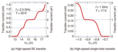
A typical result of high-speed SE transfer using the tunable-barrier transfer device is shown in Fig. 3(a) [1]. By increasing the voltage applied to the UG (VUG), we lower the electron potential of the SE island and change the number of electrons captured in the SE island. In the flat plateau regions (with current levels of 1ef, 2ef, and 3ef), an integer number of electrons is accurately transferred. In addition, we demonstrated high-speed single-hole transfer by fabricating a p-type source and p-type drain [2] (Fig. 3(b)). If radiative recombination of simultaneously transferred electrons and holes can be efficiently induced, it will be possible to realize a single-photon source with an accurate period. Furthermore, we combined the tunable-barrier SE transfer device with an SE-resolution charge sensor and evaluated the transfer accuracy by detecting the number of transferred SEs. We have so far reported that the error rate of the SE transfer is about 10−4 at about 100 MHz and that it is possible to reduce it to about 10−8 by optimizing the operating conditions [3].
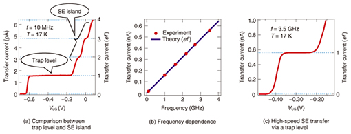
3. Silicon tunable-barrier SE transfer devices: transfer via a trap levelIn the SE transfer via the SE island, increasing the electron addition energy by scaling down the device size leads to improved transfer accuracy, but device miniaturization beyond the limitation of semiconductor nanofabrication technology is not easy. In contrast, using a naturally existing trap level with an extremely fine confinement area of less than 10 nm, which is difficult to artificially fabricate, can lead to high-accuracy operation due to its large electron addition energy. Among the silicon SE transfer devices like the one shown in Fig. 2(a), we selected a device that has a single trap level under the right edge of G1 and measured the transfer current via the trap level [4]. The trap level most likely originates from a trap at the interface between silicon and silicon dioxide. Although the voltages applied to G1 and G2 are similar to those for the transfer via the SE island, in the trap-mediated transfer, an SE is captured by the trap level from the source when the barrier under G1 is low. Then, when the barrier under G1 is high, the captured SE is emitted to the drain. Current plateaus of the SE transfer at a frequency of 10 MHz are shown in Fig. 4(a). The 1ef plateau originating from the trap-mediated transfer is much wider than the other plateaus originating from the SE-island-mediated transfer, which indicates that the trap-mediated transfer is more accurate. To perform high-speed operation, the SE capture and emission shown in Fig. 2(c) must be sufficiently fast. Detailed measurements reveal that fast capture and emission can be achieved by lowering the barrier height under G1 during the capture phase and by applying a strong electric field at the trap level during the emission phase. This can be achieved when the high-frequency signal has a large amplitude. Under this condition, the value of the 1ef plateau increases as frequency f increases, as shown in Fig. 4(b), and we achieve high-speed operation at 3.5 GHz (Fig. 4(c)). Moreover, high-resolution measurements of the transfer current at 3.5 GHz reveal that the transfer error rate is below the level (~10−3) that can be measured using a commercial current meter. In addition, we found theoretically that 1-GHz operation with an error rate of below 10−8 is possible.
4. Future workThe SE transfer via the SE island and that via the single trap level, which we have described in this article, have both advantages and disadvantages. For the trap-mediated transfer, sufficiently high-speed and high-accuracy operation is expected, but it is difficult to improve the device yield because the trap position is random. One promising way to solve this problem is to use impurity doping with a position-control technique. In contrast, the device yield of the island-mediated transfer should be better than that of the trap-mediated transfer, which is important for realizing universal standards. However, because the accuracy of the island-mediated transfer might be lower than that of the trap-mediated transfer, a temperature below 10 K is necessary. In the future, it will be necessary to evaluate the accuracy of both types of transfer at high speed by measuring the number of transferred electrons with a high-resolution charge sensor. In addition to evaluating the accuracy in more detail, we plan to conduct quantum metrology triangle experiments; we also want to apply the device to the current standards. Furthermore, we expect that the device will be able to be used for information processing based on SE manipulation. In this respect, one of the long-term goals is to achieve low-power consumption information processing by integrating the devices. References
|
||||||||||||||||||