|
|||||
|
|
|||||
       |
Feature Articles: Frontier Research on Low-dimensional Semiconductor Physics Vol. 13, No. 8, pp. 22–26, Aug. 2015. https://doi.org/10.53829/ntr201508fa5 Microscopic Probing of Crystalline Electrons Using Magnetic ResonanceAbstractElectrons in semiconductors are often referred to as free electrons, meaning that they can move freely. They are also spatially extended like a wave. On the other hand, electrons are negatively charged particles and thus repel each other. Theory predicts that at low temperatures and in high magnetic fields, electrons—in an effort to maintain a distance from one another—organize themselves. They form a regular array like the atoms in a crystal, a state known as the Wigner crystal. This article describes experiments that exploit nuclear magnetic resonance (NMR) to probe the microscopic structure of a Wigner crystal. These experiments demonstrate the capability of NMR to resolve the spatial variation of electron waves on the nanometer scale. Keywords: two-dimensional electron system, low-temperature physics, nuclear magnetic resonance
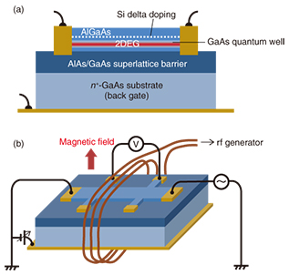
1. Two-dimensional electron system in a semiconductorMetal-oxide-semiconductor field-effect transistors, which form the basis of today’s electronics, operate by controlling the motion of charge carriers (electrons, holes) induced at the interface between silicon (a semiconductor) and silicon dioxide (an insulator). The electrons (or holes) carry electrical current by moving along the interface in response to the voltage applied between the source and drain electrodes. Since these charge carriers are confined near the interface by the electric field perpendicular to it, they can only move in the plane of the interface. Such a system is often referred to as a two-dimensional electron gas. As the term gas suggests, electrons in semiconductors can be considered to move independently between inter-particle collisions. This situation is analogous to that of electrons in a vacuum tube traveling from the cathode to the anode without collisions. However, in the solid state, the mobility of electrons depends greatly on the material and the concentration of impurities. Mobility is a quantity that describes the ability of electrons to move through a medium in response to an electric field. As a result of the continual miniaturization of electronic devices, the distance electrons travel in a transistor (the gate length) is now on the order of tens of nanometers. Research on new materials with high carrier mobility (for example, graphene or silicon germanium) is under way. This is aimed at achieving high-speed operation of electronic devices—a situation that draws parallels to Olympic sprinters on the 100-meter track. 2. Two-dimensional electron system at low temperature and high magnetic fieldAt room temperature, where electronic devices operate, the mobility of electrons is governed primarily by lattice vibrations. At low temperatures, reduced lattice vibrations generally lead to an increase in mobility. A heterostructure comprising GaAs and AlxGa1-xAs is a system in which the highest electron mobility is attained at low temperatures. The electron mobility of the sample used in this study reaches 107 cm2/Vs at a cryogenic temperature. This implies that the mean free path of electrons is as long as 100 µm. Such ultrahigh mobility requires the purity of the host semiconductor crystal to be exceedingly high; the residual impurity concentration in a material with 107 cm2/Vs electron mobility is about 1014 cm−3 (~2 ppb). Under conditions of high material purity and low temperature, electrons are able to move freely without being scattered by impurities or lattice vibrations. On the other hand, electrons are negatively charged particles and thus repel each other. Nevertheless, since electrons occupy low-energy states with long wavelengths, they tend to be spatially spread, so the repulsive interaction does not usually produce visible effects. In contrast, when a two-dimensional electron system is subjected to a strong perpendicular magnetic field, under the influence of the Lorentz force, the electrons make a circular motion (cyclotron motion) with the radius becoming even smaller than the inter-electron distance (for a sufficiently strong field). It is widely believed that in such cases, electrons—in an effort to maintain a distance from one other—organize themselves into a regular array, like the atoms in a crystal. Such a state is referred to as a Wigner crystal, named after the physicist who first predicted it. Thus far, experimental studies on Wigner crystals have relied on rather indirect information such as microwave absorption. 3. Nuclear magnetic resonance (NMR)NMR is a phenomenon in which nuclei in a magnetic field absorb electromagnetic radiation at a frequency specific to the nuclear species. It is widely used as a highly sophisticated method of spectroscopic analysis in various fields including chemistry, physics, and the medical sciences. Its principle is based on the property of nuclei (referred to as nuclear spin) that make them behave like tiny magnets. The resonance occurs at a frequency determined by the magnetic field strength and the nuclear species. In addition, the resonance frequency undergoes a tiny shift whose magnitude reflects the details of the chemical bonds and the state of the electrons surrounding the nuclei. Useful information can be obtained by measuring this tiny frequency shift (Knight shift). The reason the resonance of nuclei is affected by the surrounding electrons is that electrons also have the property (referred to as electron spin, or simply, spin) that makes them behave like tiny magnets. Electron spin can point up or down with respect to the external magnetic field. When the numbers of up-spin and down-spin electrons are unequal, the imbalance acts on the nuclei as an effective magnetic field, which shifts their resonance frequency. In NMR, measuring this Knight shift allows one to obtain information on the electrons in contact with the nuclear spins. 4. Resistively detected NMRIn standard NMR, a pick-up coil is used to detect signals produced by nuclear spins processing in an external magnetic field. However, the low sensitivity of the inductive detection makes the application of the standard NMR technique to a single-layer two-dimensional electron system unfeasible. Resistively detected NMR (RD-NMR) provides a way to overcome the issues of sensitivity, thereby enabling us to perform NMR on a two-dimensional electron system [1]. In RD-NMR, we measure the change in the electrical resistance of the sample that occurs when the frequency of the applied radio-frequency (rf) wave matches the resonance frequency of the nuclei. It also allows us to selectively detect the signal from those nuclear spins in contact with the two-dimensional electron system. The structure of the GaAs/AlxGa1-xAs (x = 0.25) quantum well sample used in this study is schematically shown in Fig. 1(a). The sample was grown by molecular beam epitaxy. Electrons are supplied from the Si delta doping layer in the upper AlxGa1-xAs barrier to the GaAs quantum well. The electron density ne is varied using the n+-GaAs substrate as a back gate. The measurement setup is shown in Fig. 1(b). The sample was processed into a 100-µm-wide Hall bar, mounted on a chip carrier, wrapped with a coil used for applying rf radiation, and cooled to 0.01 K in a dilution refrigerator. The resistance of the sample was measured using a lock-in technique with alternating current (72 Hz) in a magnetic field applied perpendicular to the sample.
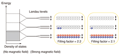
The energy level diagram of electrons in a magnetic field is schematically shown in Fig. 2. When a two-dimensional electron system is subjected to a strong perpendicular magnetic field B, the cyclotron motion of electrons is quantized, and their energy spectrum splits into a set of equally spaced discrete levels (Landau levels) designated by the orbital quantum number N (= 0, 1, 2, ...). Each Landau level is further split into spin-up (↑) and spin-down (↓) levels. The number of electrons that each spin-split Landau level can accommodate per unit area is given by nφ = eB/h, where h is Planck’s constant and e is the elementary charge. The filling factor is a quantity that represents the number of occupied (spin-split) Landau levels, and is given by ν = ne/nφ = nh/eB. As the figure shows, a filling factor of 2.2 (2.1) means that both spin branches of the lowest Landau level are fully occupied, and the lower spin branch of the first excited Landau level is 20% (10%) occupied.
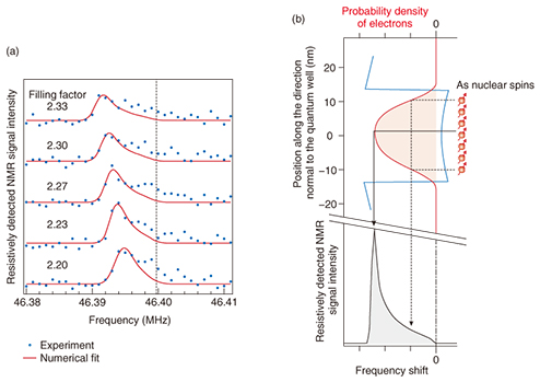
The resonance spectra of 75As taken at a magnetic field of 6.4 T are shown in Fig. 3(a). For these measurements, the filling factor is tuned in the range from 2.20 to 2.33 using the back gate. The dashed line in the figure indicates the resonance frequency of 75As nuclei observed when the quantum well is depleted of electrons. The NMR spectra taken in the presence of electrons are shifted to lower frequencies. The asymmetric line shape of the spectra with a tail on the high-frequency side reflects the variation of the probability density of electrons along the direction normal to the quantum well (Fig. 3(b)). That is, 75As nuclear spins near the center of the GaAs well and those near the AlxGa1-xAs barriers experience different effective magnetic fields from the electrons. Simulations that take into account the variation of the electron probability density along the direction normal to the quantum well, shown by the solid lines in Fig. 3(a), reproduce the experimentally observed spectra.
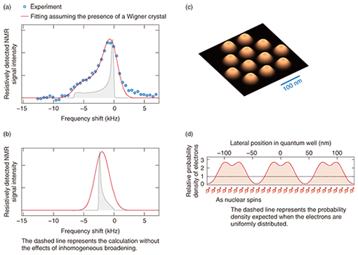
The resonance spectrum of 75As taken at the same magnetic field of 6.4 T, but with the filling factor reduced to 2.1, is shown in Fig. 4(a). (Here, the horizontal axis is taken to be the frequency shift with respect to the zero Knight shift bare resonance frequency.) Obviously, the measured spectrum does not match the simulation shown in Fig. 4(b), which is based on the assumption that the electrons are uniformly distributed in the plane of the quantum well. In contrast, simulations carried out assuming that the electrons in the first excited Landau level form a Wigner crystal (solid line in Fig. 4(a)) reproduce the experimentally measured spectrum very well. The spatial distribution of the probability density of electrons used for the above simulation is shown in Fig. 4(c). Each of the mounds arranged in a triangular lattice corresponds to a single electron. As this figure shows, at a filling factor of 2.1, the inter-electron distance becomes greater than the spatial extent of the electron wave. Consequently, it becomes energetically more favorable for the electrons to be in the crystalline state. When a Wigner crystal is formed, the probability density of electrons is no longer uniform in the plane of the quantum well, as Fig. 4(d) shows. Regions appear where the local probability density is higher or lower than that expected for the homogeneous system. In the spectrum shown in Fig. 4(a), the tail on the low-frequency side corresponds to the top of the mounds where the electron probability density is highest and the peak on the high-frequency side to the valleys where the probability density is lowest. The dip at the center of the mounds in Fig. 4(c) is a characteristic feature of the first excited Landau level wave function. The line shape of the measured NMR spectrum captures such details of the microscopic structure of the electron waves.
5. ConclusionThe results presented here demonstrate that NMR is a powerful means for probing the spatial variation of electron waves in a semiconductor. In particular, it offers a significant advantage of spatial resolution provided by nuclear spins, allowing one to obtain microscopic information about the electron wave on the nanometer scale. This opens the way to studies of other exotic phases with nontrivial spatial order. It also enables us to quantify the spatial inhomogeneity of electron density induced by randomly distributed impurities. This will be a useful technique for characterizing electronic devices facing nanometer-scale miniaturization, where eliminating device-to-device variability is a critical issue. These experiments were performed as a joint research effort between NTT and the Japan Science and Technology Agency (JST). Reference
|
||||