|
|||||||||||||
|
|
|||||||||||||
       |
Regular Articles Vol. 13, No. 11, pp. 36–41, Nov. 2015. https://doi.org/10.53829/ntr201511ra1 Microscope Integrated with Optical Connector Cleaner for Cleaning and Inspecting Optical Fiber End-faces in a Single OperationAbstractThe end-faces of optical fibers must be kept clean because unclean end-faces can cause communication errors. When optical fibers are to be connected to each other, their end-faces are cleaned and inspected using two different devices in two separate time-consuming steps. First, a fiber cleaner is used to clean each end-face, and then a microscope is used to inspect each end-face. To simplify this process, we developed a device that integrates the cleaner and the microscope into a single tool, making it possible to perform both the cleaning and inspection in a single operation without having to change tools. Keywords: optical connector, scope, cleaner
1. IntroductionOptical connectors are used for low-loss connection of optical fibers for equipment in telecommunication facilities. The end-faces of optical connectors are physically pressed together to achieve contact without gaps between the fiber cores. However, dust or other foreign material on the fiber end-faces can cause a gap or misalignment between the fibers, which can reduce the transmitted light or produce reflections and thereby degrade or disrupt communications. Moreover, foreign material can actually melt onto a fiber end-face, and the optical fiber itself can become fused if the connectors are used for high-powered light, for example, in optical line terminal video distribution or Raman amplification [1, 2]. To prevent these problems, connector end-faces should be inspected in accordance with relevant standards such as IEC*1 Standard 61300-3-35 and ITU-T*2 Recommendation L. 36. Such standards specify the permissible size and number of foreign particles in relation to the distance from the center of the fiber. Microscopic particles cannot be detected with the naked eye, so an optical connector microscope is used to photograph the fiber end-face, and the image is analyzed to determine if the inspection criteria are met. If the criteria are not met, a connector cleaner with a cleaning thread on the tip is used to clean the end-face. The end-face is then reexamined, and the inspection and cleaning processes are repeated until the criteria are met. The optical connector microscope and optical connector cleaner are separate, commercially available tools, and they are used individually in a process that involves repeated inspection and cleaning. This process can be tedious because each tool must often be switched and used a number of times. To solve this problem and increase task efficiency, we propose integrating the optical connector cleaner and microscope into a single tool, making it possible to accomplish both tasks in a single operation.
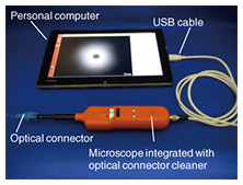
2. Configuration and operationThe configuration of the microscope integrated with an optical connector cleaner is shown in Fig. 1. The integrated device is connected to a personal computer by a universal serial bus (USB) cable. The device consists of a light source for illuminating the connector, an image sensor for photographing the connector end-face, and imaging lenses. When the tip of the device is inserted into an optical adapter into which an optical connector plug has been inserted, an image of the connector end-face is formed on the image sensor. The image acquired by the sensor is transmitted via the USB cable to the computer for display.
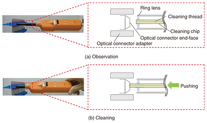
The integrated cleaner/microscope device weighs 180 grams and measures 265 × 46 × 39 mm. It is easily used with one hand in the same way as existing optical connector cleaners and optical connector microscopes. The integrated device can be used with various types of connectors, including a single fiber coupling (SC) connector, miniature universal coupling (MU) connector, and a Lucent connector (LC), by changing the tip adapter. The processes for using this device are illustrated in Fig. 2. The tip of the device is inserted into the adapter to observe the optical connector end-face (Fig. 2(a)). The cleaning step is then executed by pushing the device further into the connector adapter (Fig. 2(b)). The result of the cleaning operation can then be observed by returning the device to the original observation position. Because it is not necessary to use two separate tools, the combined process is simpler and can be accomplished in a much shorter time.
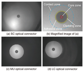
The operation of this integrated device is simple. For observation, the device is equipped with a ring lens. The hole at the center of the lens accommodates a cleaning thread, which is used to clean the connector end-face. In the observation step, only the annular lens part is used. The connector end-face is illuminated, and the image of the connector end-face that is formed on the image sensor is acquired (Fig. 2(a)). In the cleaning step, pushing the device inward causes the cleaning thread to protrude from the ring lens and press against the optical connector, thus removing foreign material. This operation makes it possible to perform both the observation and cleaning tasks efficiently. Optical systems that use a ring lens generally produce low-contrast images because the center part of the lens is missing. We designed the optical system so that it does not have this problem. The diameter of the hole at the center of the ring lens is determined by the size of the cleaning chip, and the shape of the adapter determines the aperture of the connector end-face. We took those conditions into account and optimized the lens size and the distance between the lens and the connector end-face. We thereby achieved optical characteristics that are about the same as those of a lens without a central hole. The cleaner part of the system uses a cartridge-type cleaning thread that can be replaced when it is used up. The tip of the cartridge includes the lens, so the optical system is designed with a tolerance so that positional deviation due to replacement of the cleaner cartridge does not affect the optical characteristics. 3. Example of inspecting and cleaning optical connector end-faceImages of optical connector end-faces acquired with the integrated device are shown in Fig. 3, where (a) shows the end-face of an SC connector. The dark area in the center of the image is the optical fiber, and the white area around it is the protective ferrule. An enlarged view of the optical fiber area in Fig. 3(a) is shown in Fig. 3(b). For a single-mode fiber as specified in IEC 61300-3-35, the core zone extends from the center of the fiber to a diameter of 25 μm (indicated by the red line in Fig. 3(b)). The region from 25 to 120 μm from the center is the cladding zone (orange dotted line), from 120 to 130 μm is the adhesive zone (green dashed line), and from 130 to 250 μm is the contact zone (light blue dotted line). Each zone has a particular permissible size and quantity for foreign material. We can see from the image shown in Fig. 3(b) that the observable area extends fully up to the contact zone. Observed images for MU and LC connectors, for which the ferrule diameter is smaller and the adapter aperture is smaller, are presented in Figs. 3(c) and (d). Even for these connectors, the optical fiber and ferrule can be observed in the same way as for the SC connector, meaning that detailed images can be acquired regardless of the type of connector.
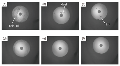
Example images before and after cleaning MU optical connector end-faces to which foreign material had adhered are shown in Fig. 4. The image in Fig. 4(a) clearly shows skin oil on the optical fiber ferrule. The ones in Figs. 4(b) and (c) show dust and lint on the optical fiber ferrule. The images presented in Figs. 4(d) to (f) show the connector end-faces after the cleaning was performed by pushing the integrated tool in and then returning it to the observation position. We can see from these figures that all of the different types of foreign materials were removed from around the optical fiber. These results demonstrate that the integrated inspection and cleaning tool operates effectively.
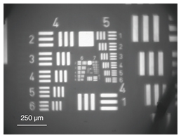
Whereas the conventional method for performing the two tasks requires an average of five steps (inspection, cleaning, inspection, cleaning, and inspection) and five tool insertions and removals, the proposed method requires one tool insertion and removal. As a result, using the integrated tool greatly shortens the total task time by eliminating most of the tool insertion and removal steps. 4. Performance evaluationWe evaluated the images acquired with this tool using the 1951 USAF*3 test target, which is often used to measure the resolution of imaging systems (Fig. 5). The test image includes lines and spaces of various widths. Analysis of the contrast of the lines and spaces in an acquired image of the test pattern showed that the imaging system can resolve line widths of 2 µm or less. Given that the IEC 61300-3-35 standard requires the ability to identify defects as small as 2 µm, this integrated tool has sufficient optical resolution for practical application.
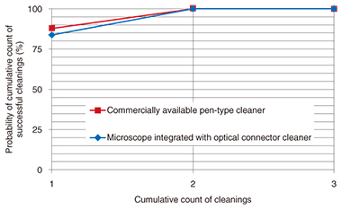
The cleaning performance of the integrated tool is presented in Fig. 6. The graph shows the test results for the number of times the cleaning operation had to be performed to meet the IEC 61300-3-35 standard. The cleaning operation was performed for an MU optical connector to which skin oil had adhered. For comparison, we conducted the same evaluation using a commercially available pen-type cleaner. We performed 50 trials for each test subject. A commercially available optical connector microscope and analysis software were used to evaluate whether the results of each trial met the criteria. The results showed that the integrated tool met the criteria with only two cleaning operations for every trial. Since the results were the same for the commercially available pen-type cleaner, we conclude that the integrated tool has the same cleaning performance as the commercially available cleaner.
5. ConclusionThe microscope integrated with an optical connector cleaner can reduce the time required for cleaning and inspecting the end-faces of optical connectors and thus reduce maintenance costs for telecommunication facilities. Evaluation of the imaging and cleaning performance of this tool demonstrated that it has sufficient optical resolution to meet the standards for optical connector inspection and has the same cleaning performance as existing optical connector cleaners. References
|
||||||||||||