|
|||||||||||||
|
|
|||||||||||||
       |
Front-line Researchers Vol. 14, No. 8, pp. 1–6, Aug. 2016. https://doi.org/10.53829/ntr201608fr1 
Research and Development that Will Be Valued 100 Years from Now―Making Dreams a Reality with Single-electron Devices Manipulating Individual ElectronsOverviewSemiconductor technology—the backbone of information and communication technology—has made amazing progress over the years, and more recently, attention has come to focus on the ultimate-level control of single electrons and single atoms using nanofabrication and crystal-growth techniques. What kind of breakthroughs can we expect from NTT’s research on ultimate electronics? We asked Dr. Akira Fujiwara, Senior Distinguished Researcher at NTT Basic Research Laboratories, to update us on recent research achievements and to tell us about his life as a researcher. Keywords: semiconductor, single-electron device, current standard
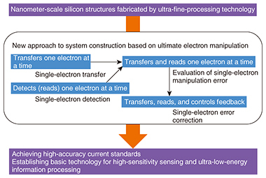
“Ultimate electronics” based on new principles and concepts—Dr. Fujiwara, please tell us about your current research activities. The computers, smartphones, and other information terminals and devices that surround us today all embed a countless number of current switches to process large amounts of information at high speed. Semiconductor technology provides the backbone for this processing. “Semiconductor” is the name given to a material that exhibits properties halfway between a metal (good conductor) and an insulator. The transistors used in integrated circuits (ICs) consist of semiconductor material, and controlling the current flowing through the ICs enables various types of information processing to be done. Up to now, the research in this area has focused on a means of downsizing IC chips and increasing the integration density as much as possible. It has so far become possible to integrate more than 100 million transistors interconnected by massive amounts of wiring on a 1-cm-square chip. However, the present mechanism for charging such wiring requires the flow of more than 10,000 electrons per one bit of information. At this rate, simply increasing the integration density will drastically increase power consumption. This is a serious issue in terms of the environment and energy-related costs. With this in mind, we are researching single-electron devices that can manipulate individual electrons with the aim of achieving devices and circuits that operate on new principles and concepts. If this can be achieved, we foresee the creation of a form of electronics having ultimate performance (in accuracy and sensitivity) and low-power characteristics that are different from the functions and performance of today’s simple electron switches (Fig. 1).
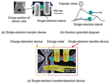
—This is certainly the seed of new technology arising from unconventional ideas. In what kind of research and in what fields would this technology be useful? The basic functions of transistors that make up an IC are often compared to the holding back and releasing of the flow of water. This analogy, however, only holds for bulk semiconductors of a sufficiently large size. In contrast, the field of research that we are currently pursuing is low-dimensional semiconductors that trap electrons in a small space. This concerns technology that confines electrons in nanometer-scale spaces by forming a laminated structure of semiconductors and insulators and contracting its dimensions using ultra-fine-processing technology. In such low-dimensional semiconductors, quantum-mechanical wave properties intrinsic to electrons and repulsive forces between electrons are particularly prominent. Here, the structure that we are dealing with is called a quantum dot, which is considered to be zero-dimensional. Within this structure, we can confine an electron in a small space and use the repulsive forces that arise between electrons to individually control electrons one by one. Such an electron-confining space is often called a single-electron island (Fig. 2). Electrically controlling the movement of electrons into and out of this single-electron island enables high-speed and high-accuracy transfer of electrons. In addition, preparing a high-sensitivity charge detection device near the island enables the detection of transferred electrons one electron at a time.
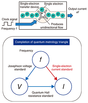
A hot topic of late is a “current standard” for accurately measuring electrical current using silicon single-electron devices that can precisely manipulate individual electrons (Fig. 3). A resistance standard using semiconductor devices and a voltage standard using superconducting devices are already in practical use, but if a current standard using a single-electron device can be achieved, it should be possible to construct a more solid electrical standards and units system.
Research on low-dimensional semiconductors has been going on for some time, and various devices have been studied. This is because it’s an attractive research theme that has much potential not only in the realm of fundamental physics but also in the field of engineering applications. We began our research on single-electron manipulation and transfer devices around the year 2000, and in March 2001, we published our research results on the first silicon-based device for manipulating elementary charge in Nature, the distinguished British scientific journal [1]. Later, in research focusing on high-speed operation of this device, we succeeded in achieving single-electron transfer by a gigahertz clock in 2008 [2]. Next, through assistance received from the Funding Program for Next Generation World-Leading Researchers (NEXT Program) of the Cabinet Office of the Japanese government, we conducted research on silicon low-power nanodevices based on the control of single or a few electrons over a three-year period starting in 2011. In this research, we developed a different approach to using an artificially fabricated single-electron island. That is, we proposed and successfully demonstrated high-speed single-electron transfer using a localized state within a semiconductor crystal to trap an electron in an even smaller space. We published the results of this research in Nature Communications in 2014 [3]. In more recent research, we have been quantitatively evaluating the accuracy of single-electron transfers and making sound progress while setting new world records in this field [4, 5]. From a “Why not?” attitude at first, to a totally committed love of research—Why did you choose physics as your research theme? Have you made steady progress as a researcher? It all started during my studies in high school and college; physics struck me as something “very beautiful.” But I also enjoyed studies related to nature and the environment, so there was a period in which I was in a quandary over which to choose as a major: physics or the environment. In the end, knowing that I was someone who liked to probe deeply into matters, physics seemed like a good fit, so that’s what I chose. However, I can’t say that this decision was a firm reflection of my career objectives. At the time, it was more like “Why not?” I think that people who can say “This is my life’s calling!” from the start are extremely rare. For this reason, I believe that it’s best to first get involved in something that you are somewhat skilled in or that you feel is worthwhile or rewarding from a social perspective. Then, by moving forward even without a clear understanding of your objectives, your calling in life should one day come into view. Looking back to the time when I entered NTT, I remember how motivated I felt as a corporate researcher on a clear career path. Today, I still have fond memories of the emotion I felt in my second year at the company, when I worked on the fabrication of transistors and actually got them to work under the instruction of my superiors and senior colleagues. In Japanese, the Chinese characters for the word “device” include the character for “child,” and the emotion that I felt on creating a device was much like the emotion one might feel on the birth of one’s child. This feeling motivated me to advance to the next step in my research career. Later on, I shifted to what is now my current line of research—the manipulation of single electrons. My research activities have not necessarily been smooth and steady, but one reason why I have been able to persevere in my research is that I have been blessed with great superiors and colleagues, and a great family too; there has always been someone to consult with whenever I hit an impasse in my work. Starting in 2004, I also spent two years in charge of recruiting staff at NTT laboratories, and because I could not do any research during that time, I became quite frustrated. However, this period proved to be a great learning experience for me on what drives people and an organization. What may appear to be a negative environment at first glance can be turned into a positive environment with the right mindset. —Where do good ideas come from in research? If there is anything that I feel to be true in my research activities up to now is that discoveries lie in laboratory experiments. I really don’t feel much insight from desktop thinking and contemplation. In the laboratory, however, I start by acquiring data, which may generate a response from me such as “Say, something is strange here!” Then, by probing deeper here and there, I can obtain many useful results. In fact, results that are different from those expected are food for an inquiring mind. This, in short, is my research style. It’s exactly at these key moments that I am particularly focused rather than in regular, everyday research. At such times, I find myself deep in thought even on the train or in the middle of a meal. When I was younger, staying up all night to work on a problem was a matter of course. I remember sleeping only six hours over a three-day period when writing my doctoral thesis. In regards to the paper we published in Nature in 2001, what supported our achievement in manipulating single electrons was our detection method for verifying whether an individual electron was actually being manipulated. This detection method was unprecedented and highly creative, and it enabled us to obtain and analyze experimental results that were not expected on the basis of previous experiments. It took about three or four years from the discovery of this detection method to the manipulation of single electrons, but I was totally absorbed in everyday experiments, and I enjoyed the entire process. Digging deeply into the cause of observed phenomena leads to the discovery of new research themes. And the criterion for assessing such a discovery is insight based on hard physics, so logical thinking is very important here. Brilliant researchers look for brilliant partners—What is important for producing good results as an active researcher? Starting in 2003, I spent a year as a researcher at the National Institute of Standards and Technology in the United States. At that time, I was already researching high-speed, high-accuracy single-electron transfer, and I thought that this institution would be a good place to move my research forward. I faced a variety of challenges there, such as assembling experimental equipment, devising measurement techniques, and coming up with good ideas. These challenges tested my competence as a researcher in an American style that evaluates not only one’s position but one’s actual abilities as well. It took several months for my abilities to be recognized, but once that happened, my research activities began to change in a big way. As my ideas came to be accepted, I began to win the confidence of those around me and to engage in lively discussions. An internationally active researcher places great importance on whom to hold discussions with. In other words, such a researcher wants to be stimulated by a brilliant partner and is always on the lookout for such a person to team up with. A researcher will not grow by withdrawing into a shell. It is imperative to seek out situations enabling contact and stimulating discussions with excellent researchers. Researchers need to challenge themselves with an open frame of mind. It is also important for a researcher to have a personality that is conducive to direct interaction in a face-to-face manner. At present, we are involved in a joint research project with the National Physical Laboratory of the United Kingdom, and I believe that making visits is one important way of earning the trust of other team members. This is my research style; when it comes to gaining the confidence of others, personality matters more than research results. Deciding whom I would like to establish a rapport with is very important. Of course, scientific credentials are necessary in a partner, but what counts in the end is whether I think that I would like to team up with that person over the long term. Moreover, to achieve breakthroughs as a researcher, it is important to maintain an interest in other researchers and research studies and to keep the channels of communication open. It is also important to ask insightful questions at international conferences and other gatherings to keep others interested in you and your activities. Even if you are unable to ask questions at a presentation for whatever reason, you can always make your voice known later in one way or another. In addition, simply chatting about common interests or hobbies is a great way of promoting communication. Such an approach can open your heart to that country’s culture and to human-interest conversations outside of research. —Can you say a few words to our young researchers? Please value intellectual curiosity and teamwork. Research results cannot be achieved by one person. In short, amassing wisdom and working hard together are essential components. You cannot achieve effective teamwork with a reserved attitude. It goes without saying that the technologies of monozukuri (manufacturing) are important, so I would like to see all of you make an active effort in accumulating and sharing know-how within your teams. There are three criteria for doing significant work in the world of basic research. The first is “Do work that can be recognized by the world.” The second is “Do work that can be evaluated and cited by other researchers in the same field.” And the third is “Do work that includes content that has the potential of being praised in the future even if it appears at first glance to be out-of-fashion research.” In other words, are you doing work that includes useful data or information that later researchers will have the urge to reference? To fulfill these criteria, keep asking yourself, “Am I falling victim to the Galapagos syndrome?” “Am I becoming a frog in the well?” Take a broad look at your research field and its history and do some objective self-analysis. Find out exactly where your research lies in the lineage or historical flow of that research. Contributing to the progress of science and technology means leaving one’s footprint on a long list of results achieved to date by other researchers. Pay homage to past research and continue to ask yourself “Am I really doing something meaningful?” —Dr. Fujiwara, what challenges will you take up going forward? We expect an electric current standard using single-electron transfer to be used as a means of directly establishing the ampere, the unit of current, which is scheduled to be redefined as part of a new International System of Units after 2018. The aim is to complete the quantum metrology triangle as a milestone toward achieving applications of this current standard. This is an experiment that aims to check the relationships among the electric current standard using single-electron transfer, the Josephson voltage standard, and the quantum Hall resistance standard. I mention here that discoverers of the Josephson effect and the quantum Hall effect each received a Nobel Prize in Physics. Our work, meanwhile, is an engineering challenge that seeks to determine the extent to which an electron can be accurately controlled. We are undertaking this work as an exit path for ultimate electronics. At present, our joint research with a team at the National Physical Laboratory of the United Kingdom is moving forward, and research projects centered particularly about Europe are progressing. Over the long term, I hope to connect this research with the further pursuit of ultimate electronics, the application of sensors, and the achievement of low-power information processing systems. In addition, while pursuing my research goals, I would like to convey my thoughts and opinions to my younger colleagues. This is not to mean that I want to push my ideas on others. Rather, I would hope to stimulate their intellectual curiosity and assist them in any way that I can. References
■Interviewee profileAkira FujiwaraSenior Distinguished Researcher, Senior Manager of Physical Science Laboratory and Group Leader of Nanodevices Research Group, NTT Basic Research Laboratories. He received his B.S., M.S., and Ph.D. in applied physics from the University of Tokyo in 1989, 1991, and 1994. He joined NTT in 1994 and has been engaged in research on silicon nanostructures and their application to nanodevices and single-electron devices. He was a guest researcher at the National Institute of Standards and Technology, Gaithersburg, MD, USA, in 2003–2004. He was a director of the Japanese Society of Applied Physics (JSAP) in 2010–2011 and a visiting professor at Hokkaido University in 2013. He received the International Conference on Solid State Devices and Materials (SSDM) Young Researcher Award in 1998, the SSDM Paper Award in 1999, and JJAP (Japanese Journal of Applied Physics) Paper Awards in 2003, 2006, and 2013. He was awarded the Young Scientist Award from the Ministry of Education, Culture, Sports, Science and Technology in 2006. He was supported by the Funding Program for Next Generation World-Leading Researchers (NEXT Program), Japan Society for the Promotion of Science, during 2011–2014. He is a member of JSAP and a senior member of IEEE (Institute of Electrical and Electronics Engineers). |
||||||||||||