|
|||||||
|
|
|||||||
       |
Feature Articles: Photonics-electronics Convergence Devices that Support AI-IoT Service Era Vol. 15, No. 1, pp. 21–25, Jan. 2017. https://doi.org/10.53829/ntr201701fa4 Very Low Power Analog IC TechniquesAbstractWe are studying the development of very compact next-generation optical transceivers by using integrated design techniques of photonics-electronics implementation. We introduce in this article the techniques used to design analog integrated circuits with very low power for photonics-electronics implementation. Keywords: integrated design, photonics-electronics implementation, very low power, shunt driving circuits
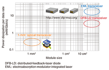
1. IntroductionTransmission capacity has grown rapidly in recent years, and further rapid increases in capacity are expected in the future with the advent of the Internet of Things and cloud computing technologies. High-speed data communication is needed in datacenters to process large amounts of traffic. However, with the increasing volume of data communication, the scale and power dissipation of datacenters is also increasing. A reduction in the size and power dissipation of optical transceivers is therefore necessary in order to reduce the scale and power dissipation of datacenters. The target power dissipation for a 1-mm2 optical transceiver is shown in Fig. 1.
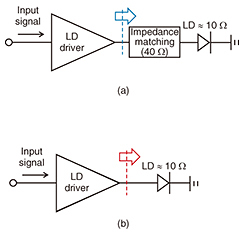
The transmission capacity of the Ethernet, the main element of the networks, has grown rapidly, and 100-Gbit/s Ethernet has been standardized. In 100-Gbit/s Ethernet, optical transceivers that have an electroabsorption-modulator-integrated laser (EML) and distributed feedback-laser diode (DFB-LD) are used. The module size of conventional optical transceivers is several square centimeters, and power dissipation per data rate is 2–20 mW/Gbit/s. Our goals are to develop a compact optical transceiver module with a size of 1 mm2 and to achieve a power dissipation per data rate of 0.5 mW/Gbit/s. To achieve these goals, we are investigating integrated design techniques for photonics-electronics implementation that take into account the impact of using optical and electrical devices. These design techniques enable the effect of photonics-electronics implementation with optical transceivers to be simulated. In addition, optical waveform simulation can be performed when the designed electrical devices drive optical devices. In this article, we introduce techniques for designing very low power analog integrated circuits (ICs). These techniques use integrated design techniques of photonics-electronics implementation and are expected to achieve very compact and low power 1-mm2 optical transceivers [1]. 2. Conventional and proposed circuitsA conventional directly modulated laser (DML)-based transmitter front-end is shown in Fig. 2(a). To match the impedance between the LD driver and the LD, an impedance matching resistor is connected to the LD in series. Therefore, extra power is consumed by the resistance. A power-efficient shunt LD driver architecture has been reported to reduce power dissipation [2]. The use of a shunt-driving circuit for the LD driver of a DML transmitter front-end results in lower power dissipation of the front-end compared to the conventional one. A DML transmitter front-end consisting of the shunt LD driver and LD is illustrated in Fig. 2(b). The shunt driver was originally used to modulate light-emitting diodes at low speed. However, recent improvements in semiconductor processes enable the shunt driver to operate with high-speed LDs. A DML transmitter front-end consisting of the shunt LD driver does not have an impedance matching resistor. Since the output impedance of a shunt driver is much higher than that of conventional drivers with an impedance matching resistor, the shunt drivers have to be placed as close to the LD as possible to avoid multiple reflections caused by impedance mismatch. Because the transmitter front-end using the shunt driver is implemented with the LD driver and LD as one, the integrated design environment of photonics-electronics implementation is necessary.
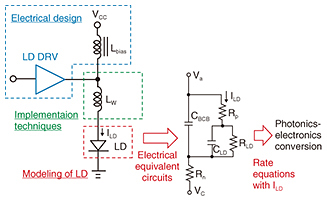
3. Integrated design techniques of photonics-electronics implementationIn this section, we discuss the elements of the integrated design techniques in more detail. 3.1 Design environmentWe created the integrated design environment of photonics-electronics implementation in SPICE (Simulation Program with Integrated Circuit Emphasis). The design environment is shown in Fig. 3 and consists of the electrical design, implementation techniques, and modeling of the LD. In modeling the LD, we first fabricated electrical equivalent circuits of the LD. Then, by inserting the LD current (ILD) of these equivalent circuits into rate equations, we were able to perform photonics-electronics conversion. The use of the integrated design environment of photonics-electronics implementation enabled optical waveform simulation to be performed in SPICE.
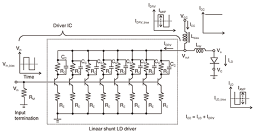
3.2 Very low power LD driverA diagram of the transmitter front-end with the linear shunt LD driver is shown in Fig. 4. In the transmitter front-end, the off-chip inductor is connected to the output terminal of the LD driver in order to apply bias to both the LD and LD driver. The anode terminal of the LD is connected to the output terminal of the LD driver by wire bonding. The inductor is denoted as Lbias. The parasitic inductance of the bonding wire is denoted as Lw, and it is about 0.16 nH in the assembly condition. The current provided from VCC (collector supply line voltage) is supplied to both the LD and the shunt driver, and the shunt driver pulls modulation current proportional to the input signal. The higher the input voltage is, the smaller the ILD becomes. Therefore, the logic of the optical signal is the inverted logic of the input signal.
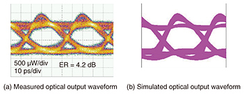
Because the output impedance of the shunt driver is high, modulation current from the driver is supplied only to the LD. The shunt driver is placed in parallel with an LD, as shown in the schematic of the transmitter front-end with the LD driver. It is configured by a common emitter amplifier with an emitter resistor; therefore, it functions as a linear amplifier. In addition, by connecting the resistor collector (RC) and common collector (CC) in parallel between the collector of the transistor and Vout, the operating points of the transistors are optimized for high-linearity and high-speed operation. The RC drops the collector voltage to set operating points of the transistors in the linear operation region. The CC, which is connected to the RC in parallel, improves the bandwidth of the LD driver. 3.3 Measured and simulated optical waveformsThe measured 25-Gbit/s NRZ (non-return-to-zero) optical output waveform is shown in Fig. 5(a). The extinction ratio (ER) is about 4.2 dB. In Fig. 5(a), the overshoot of the waveform is probably caused by the frequency of relaxation oscillations of the DFB-LD. Simulated optical waveforms are shown in Fig. 5(b). We first created an integrated design environment of photonics-electronics implementation in SPICE. Then, we carried out the simulation of the optical output waveform. As shown in Fig. 5(b), the simulated optical output waveform is the same as the measured one in Fig. 5(a). The use of the integrated design environment of photonics-electronics implementation made it possible to obtain simulated optical waveforms that were the same as the measured waveforms.
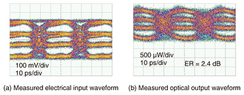
The measured electrical input 50-Gbit/s four-level pulse amplitude modulation (PAM4) waveform is shown in Fig. 6(a). The PAM4 electrical signals are unequally spaced because of the measurement setup for generating input signals. The measured optical PAM4 waveform is shown in Fig. 6(b). The ER is about 2.4 dB. The overshoot of the waveform decreases because of the high LD bias current. Changing the input bias voltage of the driver enables the linearity of the driver to be changed in response to the modulation format of the input signals. The eye openings of the PAM4 optical waveform were measured, and they show a linear response to PAM4 input signals, as shown in Fig. 6(b).
4. Future developmentWe designed a linear shunt LD driver in order to construct a low-power transmitter front-end that can operate in response to modulation formats such as PAM4. The driver was designed in an integrated design environment of photonics-electronics implementation and fabricated using our indium-phosphide (InP) heterojunction bipolar transistor (HBT) technology (ft = 290 GHz, fmax = 320 GHz). In the future, we plan to design LD drivers using a silicon CMOS (complementary metal oxide semiconductor) process in order to achieve large-scale integrated and very compact 1-mm2 optical transceivers that have a low power architecture. References
|
||||||