|
|||||||||||||||||||||
|
|
|||||||||||||||||||||
       |
Regular Articles Vol. 16, No. 11, pp. 45–51, Nov. 2018. https://doi.org/10.53829/ntr201811ra1 High-speed Avalanche Photodiodes toward 100-Gbit/s per Lambda EraAbstractWe have developed an avalanche photodiode (APD) in an effort to achieve 100-Gbit/s operation with a single wavelength (100-Gbit/s/lambda). The APD features a gap-grading layer and was set between the absorber and avalanche layers. It achieved an operating bandwidth of 42 GHz in low-gain conditions. An optical receiver made with the APD demonstrated 106-Gbit/s 4-level pulse amplitude modulation operation and 40-km optical amplifier-free transmission over a single-mode fiber under assumption of a KP4 forward error correction threshold. Keywords: avalanche photodiode (APD), 100-Gbit/s PAM4, datacenter, optical receiver
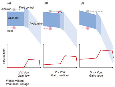
1. IntroductionThe interest in optical fiber communications systems in the last few decades has primarily been focused on long-haul systems capable of handling transcontinental communications and country-to-country communications. Such long-haul systems have included advanced optical devices used for optical communications as well as advanced modulation formats and detection mechanisms. One important example is digital coherent systems [1]. Coherent detection techniques used in combination with digital signal processors have achieved transmission distances of several thousand kilometers, and the development of densely integrated optical transmitters and receivers has enabled digital coherent systems to reach a transmission capacity of over 100 Gbit/s. Recent interest in optical fiber communications systems has been focused on short-reach applications as represented by inter/intra-datacenter networking. In 2010, 100-Gbit/s Ethernet, which utilizes a bit rate per wavelength of 25 Gbit/s, was standardized for such purposes [2], and the required bit rate per wavelength is now approaching 100 Gbit/s (100-Gbit/s/lambda). Unlike digital coherent systems, such short-reach networks are required to be low-cost and thus simple in structure. Consequently, the network systems and optical components used in short-reach networks must achieve larger capacity and longer transmission distances by using simple direct detection mechanisms and high-speed optical components. An avalanche photodiode (APD) is a key device to meet such requirements. Avalanche multiplication is initiated by electrons and holes in the APD, which provides a built-in first stage of gain of the electrical signals. Therefore, APDs obtain higher responsivity compared with the conventional PIN-PDs (positive-intrinsic-negative photodiodes), leading to higher sensitivity of the optical receivers. Thus, they effectively extend the transmission distance. To date, we have demonstrated 25-Gbit/s operation for NRZ (non-return-to zero) signals and 50-Gbit/s operation for 4-level pulse amplitude modulation (PAM4) signals by using the high-speed APDs we developed [3–5]. These high-speed APDs surpass the results of our previous examples and are aimed at achieving 100-Gbit/s/lambda operations. A gap-grading layer introduced between the absorber and the avalanche layers helped to boost the operation speed of the APD. An optical receiver fabricated with the APD achieved 106-Gbit/s PAM4 transmission over a 40-km single-mode fiber without using an optical amplifier. 2. Device design and performanceLow-gain operation must be considered when trying to boost the speed of APDs. In principle, there is a strict trade-off between the gain and the speed of the APD according to the gain-bandwidth product (GBP) rule that is governed by the material and thickness of the avalanche layer; that is, the operation speed decreases as the gain increases. Thus, one simple way to obtain high-speed operation is to operate the APD with lower gain. We employ a 90-nm-thick indium aluminium arsenide (InAlAs) avalanche layer, which provides larger GBP as well as low excess noise, in our APD. However, one problem is that a large conduction band offset exists between the indium gallium arsenide (InGaAs) absorber and the InAlAs avalanche layer. This conduction band offset is as large as 0.5 eV, which can be problematic for low-gain and high-speed operation. A schematic band diagram illustrating this issue is shown in Fig. 1.
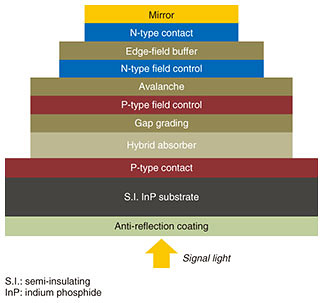
In Fig. 1(a), we show the band diagram around the absorber and the avalanche layer when the bias voltage (V) is lower than the onset voltage (Von). In this condition, the electric field in the absorber is zero, and the potential barrier caused by the conduction band offset remains. The photo-generated electrons and holes do not have drift components; thus, high-speed operation of the APD is not observed in this condition. Additional bias voltage depletes the p-type field control layer, and the electric field in the undoped absorber is invoked, as shown in Fig. 1(b). The photo-generated electrons and holes have drift components in the absorber. However, the remaining potential barrier originating from the conduction band offset prevents electrons from moving toward the avalanche layer. Consequently, high-speed operation cannot be obtained even under the V > Von condition depicted in Fig. 1(b). To eliminate the potential barrier caused by the conduction band offset, further additional bias voltage is needed (Fig. 1(c)). The additional bias voltage effectively eliminates the potential barrier but simultaneously strengthens the electric field in the avalanche layer, resulting in the increased gain of the APD. Consequently, the speed of the APD is lowered by the GBP limitation. A gap-grading layer is known to effectively relax the potential barrier [6]. We introduced a 40-nm-thick 1.1-eV indium aluminium gallium arsenide (InAlGaAs) gap-grading layer between the InGaAs absorber and InAlAs avalanche layers to relax the potential barrier that prevents the electron transport from the absorber to the avalanche layer under lower bias conditions, which can boost the speed of the APD. A cross-sectional view of the APD we developed for 100-Gbit/s/lambda (100-Gbit/s PAM4) operation is shown in Fig. 2. The APD is designed based on an inverted p-down structure [7]. The epitaxial layers, including the p-type contact, p-type absorber, undoped absorber, gap-grading, p-type field control, avalanche, n-type field control, edge-field buffer, and n-type contact layers are grown on a semi-insulating InP (indium phosphide) substrate by metal-organic chemical vapor deposition. After the epitaxial growth, we formed the triple-mesa structure shown in Fig. 2 using a wet-etching technique. Then we formed the electrodes and mirror metal by electron beam evaporation. The anti-reflection film is coated after the front-end process. Thus, the APD has a back-side illumination structure.
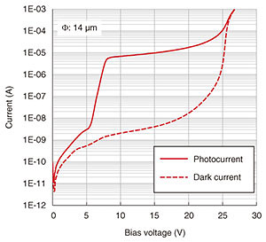
As described above, we employed a 90-nm-thick InAlAs avalanche layer. We also used a hybrid absorber consisting of 150-nm p-type and 150-nm undoped InGaAs to reduce the transit time of the electrons and holes [8]. The current-voltage (I-V) characteristics of the fabricated APD with an active diameter of 14 μm are shown in Fig. 3. The photocurrent rapidly rises from 5.5 V to 7.5 V and then increases gradually toward a breakdown voltage (Vb) of 25.4 V due to the avalanche gain. The dark current does not show any unexpected increase, indicating that the APD has no edge breakdown or other unexpected breakdown. The estimated responsivity at unit gain is 0.5 A/W against 1300-nm-wavelength optical input.
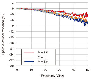
The frequency characteristics of the fabricated APD are shown in Fig. 4. A maximum bandwidth of 42 GHz was observed with a gain as low as 1.5 thanks to the gap-grading layer in the APD. A bandwidth of over 30 GHz, which is sufficient for 100-Gbit/s PAM4 operation, was maintained for the increase in gain to 3.
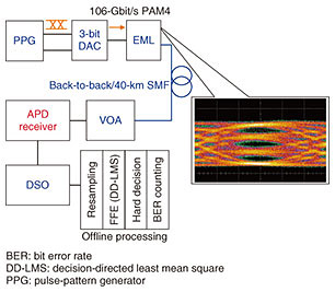
3. Receiver characteristicsTo demonstrate the 100-Gbit/s PAM4 operation of the APD, we mounted the fabricated APD into a butterfly package together with a transimpedance amplifier and conducted a transmission test with the fabricated APD receiver. The transimpedance amplifier had a bandwidth of 33 GHz, which is sufficient for 100-Gbit/s PAM4 operation. The package has a GPPO electrical output. The optical transmitter we used consisted of a 1309.49-nm-wavelength electro-absorption modulator integrated DFB (distributed feedback) laser (EML) with a launch power of +3.5 dBm [9]. The bit rate of the electrical signal that drives the EML was set to be 106-Gbit/s PAM4 by considering the overhead of the forward error correction (FEC). The 106-Gbit/s PAM4, PRBS (pseudorandom binary sequence) signal of 215-1 was generated with a 3-bit DAC (digital-to-analog converter). The optical output signal from the EML had an extinction ratio at 106-Gbit/s PAM4 operation of about 7 dB. The electrical output signal was captured by a real-time DSO (digital storage oscilloscope) with a 160-GS/s sampling rate and 62-GHz bandwidth. The transmission tests were performed with offline processing using feed-forward equalization (FFE) with a half-symbol-spaced (T/2-spaced) adaptive equalizer. No pre-emphasis on the transmitter was used. The received power was determined by the VOA (variable optical attenuator) set in front of the receiver. For the 40-km transmission test, we used single-mode fiber (SMF) with a loss of 0.33 dB/km. The measurement setup for the characterization of the APD optical receiver is shown in Fig. 5.
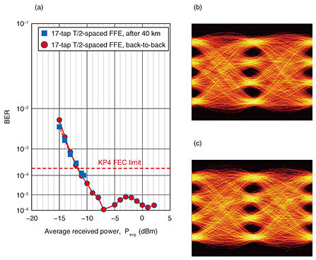
The bit error rate (BER) characteristics of the fabricated APD receiver under back-to-back conditions and after 40-km transmission are presented in Fig. 6(a). The number of taps of the FFE was set to be 17 for both conditions. In Fig. 6(b) and (c), we respectively show the equalized electrical eye diagrams of the APD receiver for back-to-back and after 40-km transmission conditions. The BER characteristics in Fig. 6(a) indicate that the fabricated APD receiver successfully demonstrated 106-Gbit/s PAM4 operation even for the 40-km transmission over SMF without an optical amplifier, as well as in the back-to-back condition. The 40-km transmission was achieved with an average received power (Pavg.) of –11.47 dBm at a KP4-FEC limit. The power penalty against the back-to-back condition was 0.32 dB. The eye diagram obtained after 40-km transmission shows no degradation from that of the back-to-back condition.
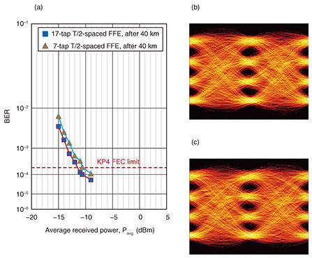
A smaller number of FFE taps is advantageous in terms of power consumption and latency by signal processing when considering the digital-signal processing used in practical optical transceivers. The BER characteristics of the APD receiver for 17-tap and 7-tap FFE after 40-km transmission are shown in Fig. 7(a). A minimum receiver sensitivity as low as –10.57 dBm was obtained, even with the 7-tap FFE. The equalized eye diagram of the APD receiver with 7-tap FFE is presented in Fig. 7(b). No significant degradation from the 17-tap condition is apparent, which indicates that the 7-tap FFE is also applicable for 40-km transmission without an optical amplifier using the fabricated APD.
4. ConclusionWe developed a high-speed APD designed for use in the 100-Gbit/s per wavelength era. We introduced an optimized gap-grading layer consisting of 1.1-eV InAlGaAs in order to achieve low-gain, high-speed operation. Thanks to the gap-grading layer, the APD exhibited a peak bandwidth of 42 GHz with a responsivity at unit gain of 0.5 A/W. A 30-GHz bandwidth was maintained for a gain of 3. The optical receiver fabricated with the APD successfully achieved 40-km optical-amplifier-free transmission for 106-Gbit/s PAM4 optical signals. These results suggest that the 100-Gbit/s/lambda era can be realized even when extending the transmission distance by using low-power-consumption, cost-effective optical components that high-speed APDs provide. References
|
||||||||||||||||||||