|
|||||||||||||||||||||||||||||||||||||||||
|
|
|||||||||||||||||||||||||||||||||||||||||
       |
Regular Articles Vol. 17, No. 2, pp. 56–62, Feb. 2019. https://doi.org/10.53829/ntr201902ra1 Highly Efficient Gate Controllability of Rashba Spin-orbit Interaction in a Gate-all-around InAs Nanowire MOSFETAbstractIndium arsenide (InAs) is a III-V semiconductor with high mobility that has attracted much attention as a next-generation semiconductor to replace the current silicon technology. At the same time, InAs is known to have a large spin-orbit interaction that causes electron spin precession even without an external magnetic field. Here, we report on an InAs nanowire metal-oxide-semiconductor field-effect transistor (MOSFET) with a gate-all-around structure, where the gate electrode is arranged coaxially with the InAs channel. We not only show that our device has good FET properties such as a high ON/OFF ratio and high mobility but also demonstrate that the Rashba spin-orbit interaction is largely controlled with a small gate voltage range, with its efficiency being ten times larger than those obtained for previously reported III-V semiconductor MOS and Schottky FETs. This indicates that our FET is promising as a prototype of a low-power-consumption spin FET, in which transistor ON/OFF is controlled as a consequence of electron spin flips. Keywords: nanowire, spin-orbit interaction, spin FET
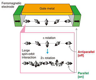
1. IntroductionGroup III-V semiconductors such as indium arsenide (InAs) and InGaAs (indium gallium arsenide) have been extensively studied as next-generation high-mobility semiconductors that can replace the current silicon (Si) technology. Another direction of research on III-V semiconductors that has been of fundamental interest for decades is their large spin-orbit interaction, which acts as an effective magnetic field and thus can rotate electron spin even in the absence of an external magnetic field. As these two research directions merged, a concept of the spin field-effect transistor (FET) was proposed by Datta et al. in 1990 [1]. In contrast to a normal transistor, in which transistor ON/OFF is defined by the changing electrical current using gate voltage, a switch for a spin FET relies on reversed spin direction in the channel, which is controlled via the spin-orbit interaction using gate voltage. The required key effect is the Rashba spin-orbit interaction, which is proportional to the applied electric field. With this interaction, the spin precession can be accessed by the gate voltage, and the device can consequently be used as a spin transistor. A spin FET is conceptually shown in Fig. 1. The spin FET is composed of ferromagnetic electrodes and an electron channel formed in a semiconductor that has a strong spin-orbit interaction. When spin is injected from one of the ferromagnetic electrodes and rotated by π via the spin-orbit interaction, the spin becomes antiparallel to the spin on the other side of the ferromagnetic electrodes, indicating that electrical current is no longer flowing.
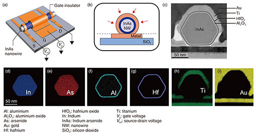
In contrast, when the electron spin rotates up to 2π due to the varied spin-orbit interaction, the spin turns so it is parallel to the spin in the other electrode, indicating that electron current has started to flow. This transistor operation resulting from spin precession can be realized by changing the gate voltage if we can use the Rashba spin-orbit interaction. This type of spin FET is expected to provide many benefits in engineering as well as to continue to be of fundamental interest. For instance, we can expect to achieve a lower-power-consumption transistor when the spin flip voltage is lower than the pinch-off voltage in normal transistors. In addition, when the spin-orbit interaction is large enough, we can integrate the spin FETs using the present Si technology. Based on this background, various III-V semiconductors have been investigated to examine whether spin-orbit interaction is indeed controlled by the gate voltage. Nitta et al. demonstrated for the first time that the spin-orbit interaction is varied by the gate voltage using two-dimensional electron gas formed in a III-V semiconductor quantum well [2]. Later, Koo et al. demonstrated that spin injection and gate control of the spin-orbit interaction occurred simultaneously for the same device [3]. Moreover, much smaller devices have been developed from quantum wire [4] and bottom-up nanowires [5–9] with the aim of achieving lower power consumption and high integration. However, the Schottky FETs and metal-oxide-semiconductor field-effect transistors (MOSFETs) used in the previous reports have not greatly improved the gate controllability of spin-orbit interaction. In this article, we report that a gate-all-around (GAA) InAs nanowire MOSFET that we recently developed has superior gate controllability of the spin-orbit interaction, which is ten times higher than that obtained for MOSFET or Schottky FETs [10]. Our demonstration will open the way toward developing low-power-consumption spin FETs. 2. ExperimentalThe GAA InAs nanowire is schematically shown in Fig. 2(a). The InAs nanowire was grown using the vapor-liquid-solid method [11]. The diameter of the nanowire is about 100 nm, and the gate length is about 3.3 µm. The GAA structure was prepared as follows. We first grow Al2O3/HfO2 (aluminium oxide: 2 nm/hafnium oxide: 4 nm) as a gate insulator around the nanowire and then put it on a pre-patterned SiO2 (silicon dioxide)/Si substrate and deposit the gate metal by an electron beam. A coaxial gate structure using a thin high-k gate insulator enables us to apply a strong electric field to the nanowire channel. The details of the fabrication procedure are described in other reports [10, 12, 13]. A TEM (transmission electron microscope) image of our device is shown in Fig. 2(c). We can see that a thin gate insulator and surrounding gate metal are formed around the nanowire. These geometries were confirmed by energy dispersive X-ray spectroscopy, which also indicates that there are no notable impurities or migration. The measurements were performed at temperatures ranging from room temperature to 1.5 K.
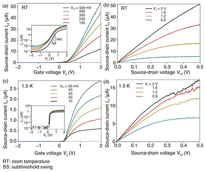
3. Results and discussionIn this section, we report the results of our experiments and explain their significance. 3.1 FET characteristicsThe transfer and output characteristics obtained at room temperature and 1.5 K are presented in Fig. 3(a)–(d). As shown in Fig. 3(a) and (c), the electrical current increases rapidly as the gate voltage increases, indicating that the device is acting as a transistor. The ON/OFF ratios extracted from these data are 104 and 105 at room temperature and 1.5 K. The subthreshold swing defined as SS ≡ dVg/dlog(Isd) is 350 mV/dec and 25 meV/dec at room temperature and 1.5 K. The mobility ranges from 400 to 1200 cm2/Vs. These values are comparable to those reported for back-gated InAs nanowires fabricated by other groups [14–16]. This demonstrates that our GAA InAs nanowire device shows good FET performance.
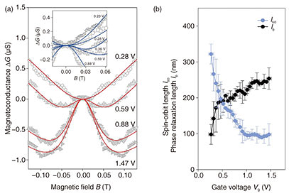
3.2 Gate controllability of spin-orbit interactionWe next investigate the strength of the spin-orbit interaction and its gate controllability. For this aim, we measure magnetoconductance to examine whether weak localization and weak antilocalization effects are observed for our device. Weak localization (antilocalization) is a quantum correction effect, which happens in the absence (presence) of the spin-orbit interaction. When the spin-orbit interaction is negligibly small, time-reversal symmetry is protected at zero magnetic field, and thus, electron waves propagating in the clockwise and anticlockwise directions produce constructive interference, leading to a weak localization. Then when the magnetic field is applied, time-reversal symmetry is broken, and the conductance is increased with the increasing magnetic field. In contrast, the opposite behavior occurs when the spin-orbit interaction is strong. At zero magnetic field, the spin flips due to the spin-orbit interaction, and thus, destructive interference occurs rather than constructive interference. This is known as a weak antilocalization effect, which results in decreasing magnetoconductance with the increasing magnetic field. Such weak localization and antilocalization effects were first considered in two-dimensional electron systems by Hikami et al. [17] and are now observed in various two-dimensional materials that possess strong spin-orbit interaction. Moreover, these effects are also observed with one-dimensional systems. In disordered one-dimensional systems, magnetoconductance (defined here as the difference ΔG from the zero-field conductance) is described with the following equation: 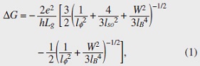 The data are analyzed using this model. In Fig. 4(a), ΔG is shown as a function of B for various values of gate voltage Vg. We can see that ΔG with respect to B shows a dip-to-peak structure with increasing gate voltage, corresponding to the transition from weak localization to weak antilocalization. Moreover, the mean free path obtained for our device is about 10 nm and is much smaller than the nanowire diameter of approximately 100 nm, so the system indeed satisfies the condition in which the model can be applied. The lines in Fig. 4(a) indicate that our data fit nicely with the one-dimensional model described by Eq. (1). From this fitting, we can extract lso and lφ, which are plotted as a function of Vg as shown in Fig. 4(b). This clearly shows that lso varies significantly with Vg and that lso becomes smaller than lφ around the crossover from weak localization to weak antilocalization.
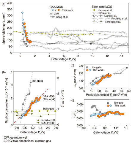
3.3 Comparison with previous reportsNext, we compare our results with those obtained for previously reported III-V semiconductors with various sample geometries. The dependence of lso on Vg measured for various InAs nanowires is summarized in Fig. 5(a). Our results plotted in different colors (blue and orange) are obtained for the same sample with different cooling times, which confirmed the robustness of the sample as well as reproducibility after thermal cycles. We can see that there is little modulation in lso for InAs nanowires with conventional back gate or top gate structures [5–9], even if a gate voltage over 10 V is applied. In contrast, our GAA and the ion-gated device developed by Liang et al. [18] show large modulation in lso within a much smaller Vg range. This is because the GAA and ion-gated structures can change the electric field over a wide range, indicating that the Rashba spin-orbit interaction, which is proportional to the electric field, varies widely with a small gate voltage. We then deduce the Rashba coupling parameter αR from lso. Here, αR is defined in the Hamiltonian representing the Rashba spin-orbit interaction,
In Fig. 5(b), αR obtained for our device is compared with those reported for one-dimensional and two-dimensional FETs that have been investigated in the context of spin FETs. The gate modulation efficiency of αR for our device is more than ten times larger than those obtained for back-gated InAs nanowire [5] and Schottky FETs fabricated from various III-V semiconductor quantum wells [2, 3]. Although our GAA MOSFET is a bit less effective than the ion-gated device, our device has great significance in that it demonstrates that such high controllability and large Rashba parameter are obtained using a MOSFET, which is much faster and more stable than ion-gated devices. We finally note the electric field ER associated with the Rashba spin-orbit interaction, which is given by ER =αR/(α0e) (α0: Rashba coefficient, α0 = 1.17 nm2 for InAs [19]). We obtain the ratio to the peak electric field E0 that is expected from the gate geometry. The results of ER vs. E0 obtained for our GAA device and the ion-gated device are plotted in Fig. 5(c). With both devices, ER is reduced more than E0 is. The ratio stays at 5% for the entire Vg range (Fig. 5(d)). This indicates that the screening effect due to the interface states that may be included in the devices is nearly the same for both devices.
4. SummaryWe demonstrated that our GAA device has higher gate controllability of the spin-orbit interaction than those obtained for standard MOS or Schottky FETs fabricated from one- and two-dimensional III-V semiconductors. The biggest advantage is that high gate controllability and the large Rashba spin-orbit interaction are obtained at a small gate voltage using a MOSFET structure. This opens the way toward realizing nanoscale spin FETs. References
|
||||||||||||||||||||||||||||||||||||||||