
You need Adobe Reader 7.0 or later in order to read PDF files on this site.
If Adobe Reader is not installed on your computer, click the button below and go to the download site.

|
Feature Articles: Network Technology for Digital Society of the Future―Research and Development of Competitive Network Infrastructure Technologies
Vol. 17, No. 6, pp. 41–44, June 2019. https://doi.org/10.53829/ntr201906fa12
Optical Fiber and Optical Device Technology for Innovative Manufacturing
Takashi Matsui, Kyozo Tsujikawa, Tadayuki Imai,
Yuichi Akage, Takashi Sakamoto, Nobutomo Hanzawa,
Yuto Sagae, Kazuhide Nakajima, and Hiroki Morimura
Abstract
Long-distance transmission of high-quality and high-power laser optics has been achieved for the first time in the world by combining the advanced optical fiber and optical device technologies developed by NTT in the optical communications field with the high-power laser processing technology of Mitsubishi Heavy Industries, Ltd. The use of laser processing technology is spreading rapidly at manufacturing sites in the automobile, aircraft, and other industries. The results of this joint research are expected to be the first step in revolutionizing the concept of manufacturing for a variety of social infrastructures through B2B2X (business-to-business-to-X) initiatives.
Keywords: laser processing, optical fiber, optical device
1. Introduction
Laser processing technology such as for metal cutting and welding is finding widespread use these days at manufacturing sites in the automobile, aircraft, and other industries. The laser beams used in laser processing can be generally divided into single mode and multi-mode*1 in terms of properties (Fig. 1). A single-mode laser beam features high directivity. The beam emitted from the optical fiber can be easily focused on a single point, making for high-precision laser processing. The output from the latest single-mode laser oscillators extends to 10 kW (about 10,000 times the optical intensity used in optical communications), which enables high-precision laser processing with good efficiency. However, the transmission distance of a single-mode laser with conventional optical fiber is limited to only a few meters.
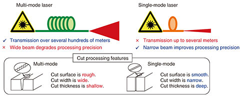
Fig. 1. Existing laser processing technology and multi-mode/single-mode features.
In contrast, a multi-mode laser beam can propagate for more than several tens of meters with existing optical fiber technology, but the wide angle of this type of laser beam emitted from the optical fiber limits processing precision. Consequently, if a 10-kW-class single-mode laser beam can be propagated over distances greater than several tens of meters while maintaining processing quality, it should be possible to greatly ease restrictions on processing location or scale of the processing target at the processing site. Furthermore, if the direction and shape of a single-mode, high-output laser beam can be freely controlled, it should be possible to control the shape in cutting and hole forming and achieve efficient overlay processing*2 (Fig. 2).
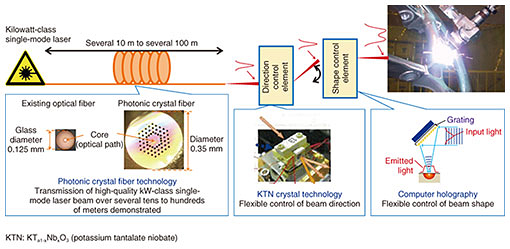
Fig. 2. New laser processing technology leveraging NTT technology.
| *1 |
Single-mode laser, multi-mode laser: In a single-mode laser, one mode of light with high directivity propagates within the optical fiber. In a multi-mode laser, in contrast, multiple modes of light propagate along various paths, which means that the laser beam emitted from the optical fiber cannot focus on a single point. |
| *2 |
Overlay processing: This is technology for improving the heat-resistance and corrosion properties of a material by welding metallic powder having desired properties on the surface of a substrate. If the shape of the laser beam used in overlay processing can be controlled to be flat and broad, the area subjected to overlay processing with one application of laser beam irradiation can be expanded. |
2. Optical fiber and optical device technology for high-power transmission
We have succeeded in transmitting a 10-kW high-quality laser beam over a distance of 30 m by optimizing photonic crystal fiber previously developed as a low-loss, high-capacity transmission medium by NTT as a high-power transmission medium [1]. Photonic crystal fiber is optical fiber that transmits light by confining it within an area surrounded by countless air holes. Precise control of the diameter and pitch of these air holes makes it possible to maintain a single mode for application to laser processing even for high power input on the order of 10 kW [2]. This joint research also involved a study on the application of potassium tantalate niobate (KTa1-xNbxO3: KTN) crystal [3], which was developed by NTT for possible application to optical switches and optical memory, and computer holography [4] to laser processing. The use of KTN crystal and computer holography here enables flexible control of the laser beam direction and shape. We expect the combination of these three technologies—photonic crystal optical fiber, KTN crystal, and computer holography—to enable 10-kW-class laser beams to be delivered to any processing site for performing flexible, high-quality, and high-efficiency laser processing.
3. Future outlook
The initiative described here is aimed at creating new added value by combining the results of research and development of competitive network infrastructure technology with technology from another industry. Going forward, we expect trials that demonstrate the potential of this technology in actual laser processing to drive its growth as a technology that can revolutionize the manufacturing sites of a variety of social infrastructures.
References
| [1] | Press release issued by NTT, “Completely Rewrite Industry’s Understanding of Transmitting High Quality Laser Processing Light over Long Distances—Innovation in Laser Processing Technology for Social Infrastructure Products by Optical Fiber Technology for Information and Communication,” Apr. 25, 2018.
http://www.ntt.co.jp/news2018/1804e/180425a.html |
|---|
| [2] | T. Matsui, K. Tsujikawa, T. Okuda, Y. Sagae, Y. Fujiya, K. Nakajima, and K. Shiraki, “High Power Beam Delivery Technology by Photonic Crystal Fiber,” 89th Japan Laser Processing Conference, 24A2-5, Osaka, Japan, May 2018 (in Japanese). |
|---|
| [3] | K. Nakamura, J. Miyazu, Y. Sasaki, T. Imai, M. Sasaura, and K. Fujiura, “Space-charge-controlled Electro-optic Effect: Optical Beam Deflection by Electro-optic Effect and Space-charge-controlled Electrical Conduction,” J. Appl. Phys., Vol. 104, No. 1, 013105, 2008. |
|---|
| [4] | T. Imai, T. Kurihara, S. Yagi, M. Endo, Y. Kurokawa, and T. Tanabe, “Orthogonal Aperture Multiplexing for Multilayered Waveguide Holographic Read Only Memory,” Appl. Opt., Vol. 42, No. 35, pp. 7085–7092, 2003. |
|---|
 |
- Takashi Matsui
- Senior Research Engineer, Access Network Media Project, NTT Access Network Service Systems Laboratories.
He received a B.E., M.E., and Ph.D. in electronic engineering from Hokkaido University in 2001, 2003, and 2008. He also attained the status of Professional Engineer (P.E.Jp) in electrical and electronic engineering in 2009. He joined NTT Access Network Service Systems Laboratories in 2003. He is involved in research on optical fiber design and measurement. Dr. Matsui is a member of the Institute of Electronics, Information and Communication Engineers (IEICE) and is an international expert for Technical Committee 86 (Fiber Optics) in the International Electrotechnical Commission (IEC).
|
 |
- Kyozo Tsujikawa
- Senior Research Engineer, NTT Access Network Service Systems Laboratories.
He received a B.S. and M.S. in chemistry and a Dr. Eng. from Tokyo Institute of Technology in 1990, 1992, and 2006. Since joining NTT, he has undertaken research on glasses for low-loss optical fibers and worked on measuring the optical properties of fiber cables. Dr. Tsujikawa is a member of IEICE.
|
 |
- Tadayuki Imai
- Senior Research Engineer, Health & Environmental-Sensing Device Project, NTT Device Innovation Center.
He received a B.E. in electrical engineering from Doshisha University, Kyoto, in 1990 and an M.E. and Ph.D. in electrical engineering from Osaka University in 1992 and 2000. He joined NTT in 1992. He has been engaged in developing optical devices including optical deflectors and holographic devices. He is a member of IEICE, the Japan Society of Applied Physics (JSAP), and the Japanese Association for Crystal Growth.
|
 |
- Yuichi Akage
- Senior Research Engineer, Health & Environmental-Sensing Device Project, NTT Device Innovation Center.
He received a B.S. and M.S. from the Department of Electrical Engineering, Osaka Prefecture University, in 1994 and 1996. He joined NTT Opto-electronics Laboratories in 1996, where he was involved in research and development of optical semiconductor devices. From 2001 to 2002 and from 2006 to 2008, he was in charge of commercializing optical semiconductor devices at NTT Electronics. From 2011 to 2016, he was engaged in facility maintenance work at the Technical Assistance and Support Center at NTT EAST. He is a member of JSAP and IEICE.
|
 |
- Takashi Sakamoto
- Senior Research Engineer, Health & Environmental-Sensing Device Project, NTT Device Innovation Center.
He received a B.A. and M.S. in multidisciplinary sciences from the University of Tokyo in 1994 and 1996 and a Ph.D. from Tohoku University, Miyagi, in 2008. He joined NTT Opto-electronics Laboratories in 1996, where he engaged in research on optical interconnections and optical packet switching. From 2004 to 2008, he studied scanning nonlinear dielectric microscopy and device applications of KTN crystals. His recent work involves KTN deflectors and their applications and high-power laser applications. He is an associate member of the Institute of Electrical and Electronics Engineers (IEEE).
|
 |
- Nobutomo Hanzawa
- Senior Research Engineer, Access Network Media Project, Advanced Media Research Group, NTT Access Network Service Systems Laboratories.
He received a B.E. and M.E. in electrical engineering and a Dr. Eng. from Yamagata University in 2005, 2007, and 2016. He has been with NTT Access Network Service Systems Laboratories since 2007, where he is researching optical fiber design, high-input-power characteristics in optical fiber, and few-mode transmission. He received the Young Researcher’s Award from IEICE in 2015. He is a member of IEICE.
|
 |
- Yuto Sagae
- Engineer, Access Network Media Project, Advanced Media Research Group, Access Network Service Systems Laboratories.
He received a B.E. and M.E. from Tohoku University, Miyagi, in 2013 and 2015. He joined NTT Access Network Service Systems Laboratories in 2015, where he has been researching optical fiber designs. He is a member of IEICE.
|
 |
- Kazuhide Nakajima
- Senior Research Engineer, Supervisor (Senior Distinguished Researcher), Access Network Media Project, NTT Access Network Service Systems Laboratories.
He received an M.S. and Ph.D. in electrical engineering from Nihon University, Chiba, in 1994 and 2005. He joined NTT Access Network Service Systems Laboratories in 1994, where he researched optical fiber design and related measurement techniques. He has been serving as a Rapporteur of Question 5 in ITU-T (International Telecommunication Union - Telecommunication Standardization Sector) Study Group 15 since 2009. He received a best paper award at the Optoelectronics and Communications Conference (OECC) 1996, a best paper award from IEICE in 2011, an achievement award from IEICE in 2012, and the Maejima Hisoka Award in 2016. Dr. Nakajima is a member of IEEE, the Optical Society (OSA), IEICE, and JSAP.
|
 |
- Hiroki Morimura
- Executive Research Engineer, Project Manager, Product Strategy Planning Project, NTT Device Innovation Center.
He received a B.E. in physical electronics, an M.E. in applied electronics, and a Dr. Eng. in advanced applied electronics from Tokyo Institute of Technology in 1991, 1993, and 2004. He joined NTT in 1993. He has been engaged in the research and development of low-voltage, low-power static random access memory and complementary metal-oxide semiconductor (CMOS) fingerprint sensors. His research interests include noise tolerant circuit design for short-range wireless communications, ultralow power circuit techniques for batteryless sensor nodes, and integrated CMOS-MEMS (microelectromechanical systems) technology. He is currently managing the product strategy planning of device technologies.
Dr. Morimura served on the program committees of the VLSI (Very Large Scale Integration) technology conference from 2011 to 2014, and the International Conference on Solid State Devices and Materials (SSDM) from 2011 to 2013. He was a special section editorial committee member of the IEICE Transactions on Electronics in 2011–2012, a Research Area Advisor of JST (Japan Science and Technology Agency) PRESTO (Precursory Research for Embryonic Science and Technology) from 2013 to 2019, and a Visiting Professor at the VLSI Design and Education Center, the University of Tokyo, from 2015 to 2017. He received the 2004 IEEE Control Systems Society Best Paper Award, the 2006 IEICE Best Paper Award, the Best Paper Award of the Symposium on Integrated MEMS Technology 2009/2015 at Sensor Symposium, and the Best Paper Award of IEEE CPMT (Components, Packaging and Manufacturing Technology) Symposium Japan 2012. He is a senior member of IEICE and a member of IEEE and JSAP.
|
↑ TOP
|


