|
|||||||||||||||||||
|
|
|||||||||||||||||||
       |
Regular Articles Vol. 18, No. 4, pp. 56–60, Apr. 2020. https://doi.org/10.53829/ntr202004ra1 Compact Silica-based 16 × 16 Multicast Switch with Surface Mount Technology for PLCsAbstractWe propose an electrical interconnection structure in which electrical connectors are directly soldered on a silica-based planar lightwave circuit using surface mount technology. A compact 16 × 16 multicast switch (MCS) having five electrical connectors was successfully demonstrated. We reduced the chip size to half that made with conventional wire bonding technology. We obtained satisfactory solder contacts and excellent switching properties. These results indicate that the proposed structure is suitable for large-scale optical switches including MCSs, variable optical attenuators, and dispersion compensators. Keywords: optical switch, planar lightwave circuit (PLC), surface mount technology (SMT)
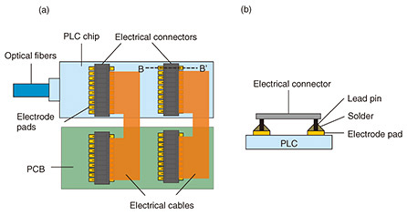
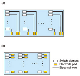
1. IntroductionOptical network automation is useful for accommodating increases in mobile and/or datacenter traffic and network restoration after serious disasters. In mobile and datacenter applications, hot and cold spots appear in different areas of networks at different times, which results in poor network resource utilization. Additional bandwidth or link assignments to hot spots will contribute to improving resource utilization, leading to a reduction in the capital expenditure for additional investment. Rapid network restoration after disasters is also required. Optical links should be changed from dead paths to live ones as fast as possible. Network automation is achieved by software-defined networking and reconfigurable optical add/drop multiplexing (ROADM) with colorless, directionless, and contentionless (CDC) functions. Multicast switches (MCSs) are enablers for the CDC-ROADM system [1–3]. Large-scale MCSs, such as those with 16 degree ports and 16 transponder ports, are important for handling a large number of signals to make the network more flexible. Silica-based planar lightwave circuits (PLCs) are suitable for large-scale optical switches because they have many advantages, such as low propagation loss, high extinction ratio, and facilitation of density integration [4–6]. M-degree ports and N-transponder ports (M × N) MCSs are composed of M × N switch elements. Each switch element consists of Mach-Zehnder interferometers (MZIs), which are driven by a heater on one of its arms through the thermo-optic effect [7]. To supply the switching power to heaters from a driving circuit on a printed circuit board (PCB), the switch elements are equipped with electrical wires and electrical pads. Although we need to densely integrate switch elements to fabricate large-scale MCSs, the large area of the electrical wiring limits their number. Thus, we need to reduce the area of the electrical wiring to enable high-density integration of the switch elements. Several compact optical switches that overcome this problem have been reported. One uses the interposer for electrical interconnection [8]. This is suitable for silicon photonics but not appropriate for larger silica-based PLCs because such PLCs have a larger chip size and the difference in the thermal expansion coefficients between a PLC and the interposer cannot be ignored. In this article, we propose an electrical interconnection structure in which electrical connectors are directly mounted on a PLC using surface mount technology (SMT). We fabricated a 16 × 16 MCS with our proposed structure. The chip size of the PLC was successfully reduced to half that of a conventional chip using the bonding wire method. We obtained excellent switching performance. 2. Proposed structureFigure 1(a) shows a top-view schematic of our proposed structure. The electrical connectors are directly mounted on the silica-based PLC chip. The lead pins of the electrical connectors are soldered to the electrode pads on the PLC surface, as shown in Fig. 1(b), which is a cross-sectional view at B-B’ in Fig. 1(a). The PLC and PCB are connected to each other with electrical cables, such as flexible print circuits (FPCs). Figure 2 shows the designs of electrical wiring in the PLC chips of an M × N matrix or MCS, which are for a conventional electrical connection structure and our proposed structure, respectively. Conventionally, as shown in Fig. 2(a), a PLC and PCB have been connected electrically using a general wire bonding method. Electrode pads are arranged on the edge of both the PLC and PCB to bond them with gold wire. In this design, long electrical wirings are arranged from each heater to each electrode pad on the edge of the PLC. Thus, the arrangement of the electrical wiring on the PLC becomes complicated and its area increases with the number of switch elements, which limits the miniaturization of the chip. On the other hand, the arrangement of electrical wiring with the proposed structure is simple, as shown in Fig. 2(b). As the electrode pads can be placed near the switch elements, the length of electrical wiring can be shortened. Therefore, this structure enables us to reduce the area of the electrical wiring and integrate the switch elements more densely. The proposed structure also offers advantages such as automatic fabrication because the electrical connectors can be mounted on the PLC using general SMT widely used in the assembly of electrical devices. The proposed structure also makes it possible to mount the connectors automatically at the wafer level, making it suitable for mass production.
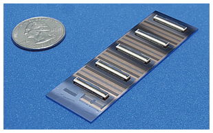
3. Experiment3.1 FabricationFigure 3 shows a photograph of the 16 × 16 MCS chip with the proposed structure. The chip was fabricated using the conventional silica-based PLC fabrication process. The 256 switch elements, consisting of MZIs and heaters, are regularly arranged in the PLC, and each heater is connected to the electrode pad with electrical wires. The electrical wires are shorter than those in a conventional PLC switch with wire bonding because the electrode pads are placed near the switch elements. Therefore, the area of the electrical wiring in the chip is greatly reduced. The chip size is 23.5 × 72 mm. We estimated that it is two times smaller than a conventional 16 × 16 MCS with wire bonding. After PLC fabrication, five electrical connectors are mounted on the PLC chip with solder using SMT at the 6-inch wafer level. After AgSnCu (Ag: silver, Sn: tin, Cu: copper) solder paste has been patterned on the electrode pads by screen printing, the electrical connectors are mounted and soldered by the standard reflow process. As there are 256 heaters in the 16 × 16 MCS chip, we mount five electrical connectors on it. Since general electrical connectors have approximately 50 to 80 pins, we can construct a large-scale MCS by increasing the number of mounting electrical connectors. Therefore, our structure is scalable for constructing much larger MCSs.
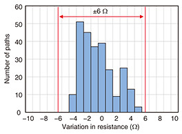
3.2 Electrical characteristicsWe measured the resistance of the 256 switch elements by connecting the PLC and PCB with an FPC, as shown in Fig. 1(a). Figure 4 shows the variation in the average resistance of the 256 heaters. This variation includes the variation in the heaters, electrical wires on the PLC, soldered connection parts between the electrode pads in the PLC and PCB and the lead pins of the electrical connectors, and the contacts between the FPC and electrical connectors. The variation in the average resistance was less than ±5 Ω and 3σ (σ: standard deviation) was 6.8 Ω. In our switch module, the variation needs to be less than ±6 Ω to satisfy the need to keep the variation in insertion loss of all switch elements within ±0.1 dB. Thus, this result indicates that satisfactory connections were obtained for all soldered parts. We estimate that this variation in the resistance resulted in the variation in the length of the electrical wires. Thus, this variation in switch resistances can be reduced by changing the width or length of the electrical wires.
3.3 Optical characteristicsWe evaluated the switching characteristics of all 256 connections from 16 degree ports to 16 transponder ports at the wavelength of 1550 nm. By measuring transmission changes with electric power applied to the heater, we obtained clear switching characteristics for all 256 paths. Figure 5(a) shows the measured on- and off-state transmittance for all 256 paths. The average switching power per switch element was 0.24 mW. It was clearly observed that all the paths operated correctly, proving that our proposed structure works well. Figures 5(b) and (c) show a histogram of the insertion loss and extinction ratios for all 256 paths. The average insertion loss and standard variation were 15.2 and 1.0 dB, respectively. The insertion loss includes intrinsic loss of 12 dB. Thus, the excess loss is as small as 3.0 dB on average. The average and variation in the extinction ratio were 53 and ±5 dB, respectively. As described above, all the paths operated correctly, proving that the proposed structure works well.
4. ConclusionWe demonstrated a compact 16 × 16 MCS using our new electrical interconnection structure based on SMT. Five connectors are soldered directly to the PLC by the standard reflow process used for electric devices. We successfully reduced the chip size to 23.5 × 72 mm, which is two times smaller than a conventional chip with wire bonding. We obtained satisfactory solder contacts and excellent switching properties. These results indicate that our proposed structure is suitable for large-scale MCSs and this new electrical interconnection method with SMT can be applied to other silica-based PLC devices. References
|
||||||||||||||||||