|
|||||||||||||||||||||||
|
|
|||||||||||||||||||||||
       |
Front-line Researchers Vol. 18, No. 8, pp. 1–6, Aug. 2020. https://doi.org/10.53829/ntr202008fr1  Exploring New Fields and the WorldOverviewIn April 2020, NTT formulated a technology roadmap for implementing the Innovative Optical and Wireless Network (IOWN). Photonic disaggregated computing, one of the key technologies that make up IOWN, is generating great interest as a new architecture that shifts from the conventional physical-server-oriented computing platform to a serverless computing platform based on photonic data planes. We asked Masaya Notomi, a senior distinguished scientist at the Nanophotonics Center of NTT Basic Research Laboratories conducting basic research on enabling photonic disaggregated computing, about his current research efforts and attitude as a researcher. Keywords: nanophotonics, photonic crystals, all-optical switch
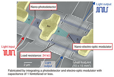
Announcement of research results that attract attention from around the world—Could you tell us about the research you are currently working on? Currently, I am working on two themes. One is developing opto-electronic integrated processors using integrated nanophotonics*1 by further advancing research on photonic crystal devices that operate with the world’s lowest energy consumption, which we achieved about 10 years ago. By constructing a photonic network on a chip, we are trying to break through the limits of conventional integrated-circuit technology in terms of processing capacity, delay, and power consumption. By fully using the nanophotonics technology we developed thus far, we have devised the following three devices: (i) a nano-photodetector that has the potential to convert optical signals to electrical signals with zero electric energy consumption; (ii) nano-electro-optic modulator that performs electro-optical conversion with only 6% the energy consumption of a previously reported modulator; and (iii) optical transistor that combines these devices [1] (Fig. 1).
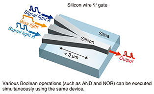
A processor is generally composed of a combination of many logic-operation circuits, each of which is composed of a combination of logic gates, and each gate is composed of a combination of transistors. After developing the optical transistor, we successfully demonstrated the world’s first low-loss, high-speed operation of a small optical logic gate called “Ψ (psi) gate” that operates by optical interference only. We published a paper about this in March 2020 [2] (Fig. 2). With this technology, typical logic operations (AND, XNOR, NOR, etc.) can be carried out with ultralow delay in a wavelength-independent manner by using only a single Ψ gate. By this gate integrating with a high-speed optical modulator, it is possible to simultaneously carry out different operations to each wavelength channel (wavelength-division multiplexed parallel computation). Coordinating various devices, such as operation circuits, will make it possible to devise the first opto-electronic integrated processor with low latency and low power consumption that has specific functions.
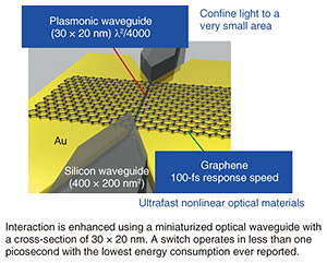
The second theme, which is a more fundamental research, is on novel optical phenomena. Part of this research is being conducted jointly with a laboratory of the Tokyo Institute of Technology, at which I also hold a post. New nanoscale materials (nanomaterials), such as carbon nanotubes, have recently been discovered and have been shown to have various functions. By applying nanophotonics technology to these nanomaterials and generating interactions between nanomaterials and light, it has become possible to discover various new phenomena. For example, simply placing an InAs/InP (indium arsenide/indium phosphide) nanowire on a silicon photonic crystal*2 will create an optical nano-resonator at that point. We have also succeeded in demonstrating laser oscillation by using nanowires with a size less than the wavelength of the laser. Moreover, by combining graphene*3, which has excellent nonlinear optical characteristics, with an extremely small nano-optical waveguide (plasmonic*4 waveguide), we have demonstrated an all-optical switch that operates in the ultrafast range (less than one picosecond) with low energy consumption [3] (Fig. 3). What’s more, topological photonics, which applies topological-field theory*5 in solid-state physics to optics, is a new field of optics and expected to produce novel physical properties that we do not know what to do with yet. In this field, we theoretically discovered that a photonic topological insulator can be formed by current injection. This last topic is a more or less basic research, in which we cannot anticipate what will be discovered; thus, it is very exciting.
Our research is one of the technical directions outlined in the “Technology Development Roadmap for Realizing the IOWN (Innovative Optical and Wireless Network) Concept” announced in April 2020 [4]. To develop a cloud-computing infrastructure that seamlessly spans multiple datacenters, thereby contributing to achieving computing scaling across device, edge, and center cloud, we are engaged in basic research related to high-speed distributed-computing methods that use the ultrabroadband and low-latency communication on the All-Photonics Network.
Find interesting seeds, have fun, and communicate how interesting your research is with other people—Could you tell us what you value when you do research? What I value most when doing research is whether a theme is interesting. For example, we could not see any outcome when we started researching nanophotonics, but future applications were in sight after thoroughly investigating them. We are working on themes as a team, so if we find an interesting seed, someone on the team will substantiate it. All our research activities may seem successful because we have published the results of what we succeeded in pursuing, but, of course, some of our activities were failures. Sometimes we are more likely to fail. That’s why research activities cannot continue unless the researchers themselves find them interesting. Also, unless other people think our activities are interesting, it may be difficult for the value of our research to be socially recognized. I sometimes talk with researchers in Europe and the United States at academic conferences. If I can’t tell them what’s interesting about my research and share my enthusiasm with them, I don’t think they will become interested in it. Moreover, research activities will change according to phases and levels. It has been more than 10 years since my last interview. Last time, on finding new phenomenon, I first thought of combining nanophotonics and devices. The research phase and level then changed to applying nanophtonics to circuits then to processors. It took us about five years to ensure that nanophotonics could be useful, and since we knew what we could use, I discovered another interesting aspect of the phenomenon. It is said that matters progress like a spiral, but once certain research is complete, the process of rethinking and setting up is repeated. The interestingness is scattered throughout that process. When you are young, your research theme covers a narrow range; however, after doggedly doing your best, you gradually become able to handle several themes in parallel. Through close inquiry, targets of interest will appear one after another. However, I think that we should not let our research diverge according to our interests only. I also think that the number of things that we can handle will increase because we are working as a team. Therefore, we must be able to communicate how fascinating and interesting our research is. The more people you have on your team, the more ideas you will have. —Is there anything you have done to improve yourself as a researcher? I’ve been deliberately working on a new theme. Large and complex themes, especially, will not be pursued if we do not consciously work on them, which I think is an essential attitude a researcher should have. Researchers at NTT, especially those involved in basic research, may have a medium- to long-term perspective, and they can continue their research at their own pace and focus on the same subject throughout their time at NTT without any short-term pressure on producing results. However, if a researcher continues to study the same subject for a long time, he/she may get bogged down. At such times, I think we must have the courage to change the theme. I also think if we don’t have the initiative to search for new themes, cross fields, or change departments, our feelings about and sensibilities of what is interesting will fade. Now, the research that I am currently working on is aimed at fabricating an opto-electronic processor using integrated nanophotonics. We have been able to generate original results by collaborating with researchers in other fields. In the past, I didn’t think I would collaborate with people in the electrical and circuit fields during my research; however, I have recently been working with researchers who originally had no experience in my research field. Such a situation is somehow strange but very interesting. For example, different fields use different language. So, we first desperately speak in our own language, thus we cannot understand each other at all. After we talk many times, however, we start to understand each other. We learn the language of the other field and use it to talk about our own field. I find this process of gradually developing common words very interesting. I think it is important to continue our research while receiving this stimulus. If we don’t pay attention to that stimulus, it will disappear, and we will not be able to produce original results. —What does it mean to be a researcher? What is required for researchers today? I think a researcher can be quite different from other professions. In most other professions, wages are paid for the results of the work; however, researchers are paid for what they are doing. Even if a researcher does not produce results; for example, even if they don’t achieve anything for 10 years, it is difficult to evaluate their research work as meaningless. In addition, I think that if rewards are paid only for achievements, it will be difficult to maintain motivation, especially in the case of basic research with a long research span, which wouldn’t allow us to even talk about interesting research. Given this consideration, it is necessary for researchers to engage in research every day with the awareness that they are rewarded for their research activities. Even if we do not know whether our research results will contribute to society, it is important to take up the challenge with the spirit and belief that we will contribute, and that is why I think being interested is an essential element of research activities. Then, as I mentioned above, we will be asked to explain more about our research. It is important that our research be known as useful to society; it is even better if that research is reported in the mass media. Moreover, it would be great if we could share the interestingness of our research and the excitement about our daily research with the general public, but that is probably too much to ask. Let’s venture into other fields and the world—Please give a word to all our young researchers. The number of research topics and fields has increased considerably, so it is difficult to follow them all; even so, I think it is very important to consciously attempt to understand other fields. It’s easy to access information online, and young people, namely, “digital natives,” are more accustomed to using the Internet than my “digital immigrant” generation, so I think they work in a good research environment. Unfortunately, I feel that over the past five years, young Japanese researchers have not as aggressively entered new research fields. Around the world, new fields and research themes are emerging one after another, and information about them is undoubtedly available, but young Japanese researchers have not ventured into these fields. I think that there are many excellent Japanese researchers, but in this situation, they will not able to obtain original results, and they will just rehash old ones. Therefore, I’d like our young researchers to watch out for new trends, be sensitive to information, and work hard. So how do we take up a new research theme or field? One way is to knock on the gates of overseas research institutes. When I was in my mid-thirties, about 10 years after I started research, my boss told me, “Find your own research theme no matter what you do.” So, I went to study in Sweden for a year, which was a very good experience. I think it’s beneficial to take the opportunity to go abroad when you are young. In the past, being in academia in Japan enabled us to understand worldwide research trends, but the situation for giving research presentations is changing and includes online conferences. That’s why I think it is necessary to go to international conferences held overseas and research institutes to directly communicate with many researchers. It is also important to write papers and publish research results. Needless to say, peer review in the process of publication gives us a new perspective since the readers are also researchers. Ambiguousness may be allowed when reporting your achievements in your laboratory. When writing a paper, however, you must make the points of your arguments clear, so it helps to clarify your thoughts in the process of writing. Moreover, considering various items through that argument may lead to new discoveries. You are probably curious about the number of citations your paper gets, but you should also be interested in how your paper was cited. When the paper is published, it is the result of what you thought of, but it then can be further developed, changed, and expanded through the interpretation of the other researchers who cite it. My paper titled “Theory of Light Propagation in Strongly-modulated Photonic Crystals: Refraction-like Behavior in the Vicinity of the Photonic Band Gap”—published in 2000 [5]—was cited in many other papers, and it became clear that antimatter affects certain physical phenomena. After that, the interpretation of my results spread further. The number of papers you write each year depends on your research topic and environment, so you may not need to set a standard. In some institutes, like universities, the number of papers is significant, in others, such as in-house research institutes, the focus is on business promotion rather than papers. However, you won’t necessarily finish your research life at the place you are now. Therefore, it is better to write papers so that you can be a researcher who can go anywhere and can clarify your research work and purpose. —How will you proceed with your research activities in the future? There were many prestigious research institutes but most do not exist today; for example, Bell Labs in the USA. NTT laboratories, in contrast, uniquely focus on everything from basic research to applied research. One can take up large research challenges because he/she has basic research and applied research in one institute. I want NTT to be a role model for other research laboratories as the number of laboratories that are firmly engaged in basic research decreases. However, I don’t think we should be satisfied with doing research that general universities can do. I also have a laboratory at the Tokyo Institute of Technology, so I’d like to focus on nurturing the next generation of researchers. I think that the fields I’m working on will be enriched if I convey the knowledge I have accumulated and nurture those researchers. I can’t accomplish everything myself, so I want new people to take the lead. References
■Interviewee profileMasaya NotomiSenior Distinguished Scientist, Nanophotonics Center, NTT Basic Research Laboratories. He received a B.E., M.E., and Ph.D. in applied physics from the University of Tokyo in 1986, 1988, and 1997. He joined NTT in 1988 where his research has focused on controlling the optical properties of materials/devices using artificial nanostructures (quantum wires/dots and photonic crystals). In addition to his work at NTT, he has also been a professor at the Department of Physics, Tokyo Institute of Technology since 2017. He received the IEEE/LEOS Distinguished Lecturer Award (2006) from the Institute of Electrical and Electronics Engineers/Lasers & Electro-Optics Society, the JSPS prize (2009) from the Japan Society for the Promotion of Science, a Japan Academy Medal (2009), and the Commendation for Science and Technology by the Japanese Minister of Education, Culture, Sports, Science and Technology (2010). Dr. Notomi is an IEEE Fellow and a member of the Japan Society of Applied Physics (JSAP), the American Physical Society (APS), and the Optical Society (OSA). |
||||||||||||||||||||||