|
|||||||||||||||||||||||
|
|
|||||||||||||||||||||||
       |
Regular Articles Vol. 19, No. 5, pp. 74–82, May 2021. https://doi.org/10.53829/ntr202105ra1 Ultra-high-speed 300-GHz InP IC Technology for Beyond 5GAbstractA 300-GHz-band 120 Gbit/s wireless transceiver (TRX) is presented using our in-house indium phosphide (InP) high-electron-mobility transistor (InP-HEMT) technology. A 300-GHz power amplifier (PA), which is the key component in the TRX, was developed using the backside DC line (BDCL) technique to increase its gain and output power. The measured maximum gain and saturated output power are respectively 20.5 dB and 12 dBm. The 300-GHz-band TRX was fabricated using this PA. The TRX achieves high data rates of 124 and 120 Gbit/s under back-to-back and 9.8-m-link-distance wireless data transmission conditions. To the best of our knowledge, these are the highest data rates among reported 300-GHz-band TRXs. Keywords: 300 GHz, InP-HEMT, power amplifier
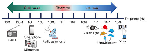
1. IntroductionA terahertz (THz) wave is an electromagnetic wave located in the boundary of a radio wave and light wave, as illustrated in Fig. 1. Its frequency range is from around 300 GHz to 10 THz. It had been very difficult to generate and control THz waves due to the lack of semiconductor devices working in this high frequency region. Due to the progress of miniaturization technique for semiconductor devices (transistors), the operation frequency range of cutting-edge transistors is above 1 THz [1]. By using these high-speed transistors, the applications of THz waves, such as wireless communication [2] and imaging/sensing for security [3], are being extensively investigated. High-speed wireless communication is one of the major applications of THz waves due to their broad bandwidth. In the next generation of the fifth-generation mobile communication system (5G), called beyond 5G or 6G, a data rate of more than 100 Gbit/s is considered necessary. The 300-GHz-band is considered suitable for beyond 5G due to its relatively low atmospheric attenuation (< 10 dB/km) in the THz region. In this article, we report on the recent achievements with a 300-GHz-band power amplifier (PA) we developed using our in-house indium phosphide (InP) high-electron-mobility transistor (InP-HEMT) integrated circuit (IC) technology and over-100 Gbit/s wireless transceiver front-end (TRX) fabricated using this PA.
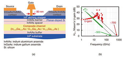
2. InP-HEMT technologiesInP device technologies to fabricate 300-GHz-band ICs for TRXs are introduced in this section. The mandatory device technology for 300-GHz-band ICs is the high-speed transistor InP-HEMT. There are two frequently used figures of merit for high-speed transistors, i.e., transition frequency (fT) and maximum oscillation frequency (fMAX). The former is an index to show the maximum switching speed and the latter shows the maximum power-amplification frequency of the transistor. Therefore, fT is related to the operation frequency of a switching circuit such as a passive mixer and multiplier, whereas fMAX is related to the operation frequency of active circuits such as an amplifier and oscillator. A cross-section schematic of our in-house InP-HEMT is shown in Fig. 2(a). Generally, InP-HEMTs have superior high-speed characteristics by using the high-electron-mobility material indium gallium arsenide (In0.53Ga0.47As), which can be epitaxially grown (i.e., lattice-matched with InP) on InP substrate as their channels. With our InP-HEMT technology, to attain higher speed than with normal InP-HEMTs, a composite channel composed of In-rich In0.8Ga0.2As and lattice-matched In0.53Ga0.47As [4] is applied using InGaAs because the ratio increase of In can enhance its electron mobility. The gate length also decreased to 80 nm to shorten the electron transit time in the channel and enhance both fT and fMAX. The measured current gain (H21) and maximum unilateral gain (U-gain) of this InP-HEMT are plotted in Fig. 2(b), showing high fT and fMAX of 300 and 700 GHz, respectively.
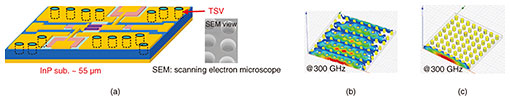
To fabricate 300-GHz-band ICs, it is not sufficient to have high-speed transistors. The problem specific to THz ICs caused by a substrate mode as described below should be managed. A substrate mode is an electromagnetic wave that propagates in substrate. When the substrate thickness is the same order of wavelength, the substrate mode can propagate. The commercially available InP substrate thickness is around 600 μm and the wavelength of a 300-GHz-band signal in InP substrate is below 500 μm. Therefore, a substrate mode can be guided, causing unwanted coupling between some ports of THz ICs, e.g., coupling of input and output ports of the amplifier by the substrate mode can cause the oscillation of that amplifier. To cut out the propagation of the substrate mode, substrate thinning and through substrate via (TSV) are applied in the back-end IC process [5, 6]. By using substrate thinning, the thickness of the InP substrate is reduced to 55 μm, as shown in Fig. 3(a). TSVs are densely formed over the entire substrate area to reduce the substrate space that can support the propagation of substrate modes, as also shown in Fig. 3(a). The TSV density is critical to sufficiently cut out the substrate mode. Figures 3(b) and (c) shows a 300-GHz substrate-mode propagation calculated using an electromagnetic simulator when the TSV pitch (TSV edge-to-edge distance) is set to 100 and 50 μm, respectively. By using the 50-μm pitch, the substrate mode is sufficiently cut out. Therefore, around the 50-μm pitch, the TSV layout is used in the 300-GHz-band PA, as described in the next section.
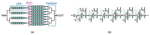
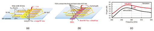
3. 300-GHz PAThe important characteristics of the PA for TRXs are gain and output power to achieve a sufficient signal-to-noise ratio (SNR) of 300-GHz-band wireless communication. A schematic of the PA is shown in Fig. 4(a). It is composed of unit power amplifiers (UPAs) consisting of six-stage common-source amplifiers using the InP-HEMTs described in Section 2, as illustrated in Fig. 4(b). This six-stage cascading design produces high gain of more than 10 dB for a UPA at 300 GHz. The inter-stage matching for each common-source amplifier stage in a UPA is designed to have small loss by using the low impedance matching technique [7, 8]. To achieve both high gain and high output power in a UPA, the first three stages are designed with high-gain two-fingered HEMTs, and the latter three stages are designed with four-fingered HEMTs that have higher power handling and slightly lower gain than two-fingered ones, as shown in Fig. 4(b). The PA has eight-paralleled UPAs in its output stage to achieve high output power by combining the output power of each UPA. In the middle part of the PA, the backside DC line (BDCL) is used to also achieve high gain and output power. The role of the BDCL technique is explained as follows.
The PA shown in Fig. 4 (a) uses many transistors due to the series-amplifier stage in a UPA and paralleled fashion in the PA output stage. In such a case, a very wide (several hundred microns) DC line should be used to support large total drain current (~ 1.8 A), which is necessary to operate many transistors. Therefore, the typical layout of this PA is similar to the one shown in Fig. 5(a). Long radio frequency (RF) transmission lines (TLs) should overlap the wide DC line. These long RF TLs have high transmission loss in a high frequency range, such as the 300-GHz band, and reduce the gain and output power of the PA. To address this issue, the BDCL is introduced. With this introduction, the wide DC line is put on the backside of the InP chip (Fig. 5(b)). Thus, the overlap between the RF TLs and wide DC lines in Fig. 5(a) is eliminated and the gain and output power of the PA increases. The simulation comparison of the PA gain is shown in Fig. 5(c). By using the BDCL, the simulated gain increases by around 3 dB over 280–320 GHz.
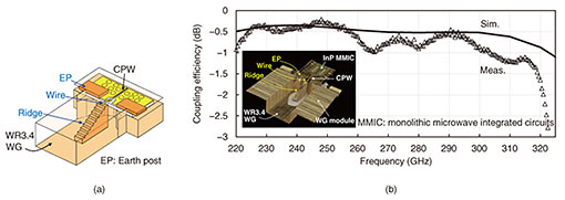
The PA chip is difficult to handle for implementation in TRXs. To improve ease of handling, the IC packaging in a robust metal module is important. In the 300-GHz band, the widely used media is a rectangular waveguide (WG). Therefore, we developed a PA module with WG flanges for its input and output. The critical component for this PA module is the transition between the PA IC and WG. A ridge coupler [8, 9], shown in Fig. 6(a), is used as the transition. It translates the guided mode of the WG to the coplanar waveguide (CPW) mode, which is used in the PA IC. A step-wise metal component formed on the center part of the WG, called a ridge, gradually transforms the impedance and forms of electromagnetic wave between the WG and CPW. A bondwire is used to connect the ridge and IC CPW pad. A three-dimensional photograph and simulated and measured coupling efficiencies of this ridge coupler are shown in Fig. 6(b). The coupling loss is very small, less than 1 dB over 220–303 GHz.
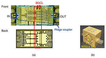
The PA IC and module were fabricated using the techniques described above, as shown in Figs. 7(a) and (b). The BDCL placed in the vicinity of the center part of the PA chip is electrically isolated from the DC ground by the mask and etching process in the InP back-end process, as shown in Fig. 7(a). The fabricated PA module has WR3.4-band (220–325 GHz) WG flanges for its input and output, as shown in Fig. 7(b).
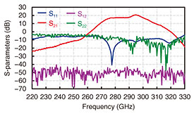
The characteristics of the PA module were evaluated through small- and large-signal measurement. We first conducted a small-signal measurement using a vector network analyzer (VNA) and WR3.4-band frequency extenders. The measured S-parameters are shown in Fig. 8. It achieved a maximum gain (S21) of 20.5 dB at 295 GHz and broad bandwidth. The reverse transmittance (S12) is very small, less than –40 dB over the full WR3.4 band. Therefore, the PA module is very stable. This is because the InP back-end process shown in Fig. 3 successfully reduces substrate-mode propagation. The measured gain matches the simulated gain in Fig. 6(a).
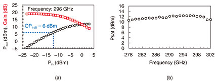
Next, we measured large signal characteristics. The input-output characteristics are shown in Fig. 9(a). The PA module achieved high saturated output power (Psat) and output 1-dB compression point (OP1dB) of 6 dBm. The measured frequency dependence of the Psat is shown in Fig. 9(b). The Psat is larger than 10 dBm over 278–302 GHz. These high-power characteristics are derived from BDCL technique and the low-loss ridge coupler, as described above.
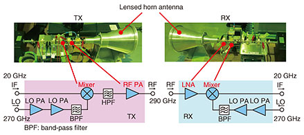
4. 300-GHz-band TRXWe fabricated a 300-GHz-band TRX using the PA module described in Section 3. The TRX has a heterodyne architecture. The transmitter (TX) consists of a frequency converter (mixer), local oscillation (LO) PAs to operate these mixers, and an RF PA (same as the one described in Section 3). The receiver (RX) is composed of a mixer, LO PA, and low noise amplifier (LNA). The intermediate frequency (IF) and LO frequency are set to 20 and 270 GHz, respectively. The fundamental mixer [8, 10] using our in-house InP-HEMT technology is used for both TX and RX. In the RX, the same PA discussed in Section 3 is used as the LNA. This TRX uses the upper-side band for the RF (290 GHz). High-gain (50 dBi) lensed horn antennas were used for both TX and RX in the wireless-transmission experiment discussed later. The lower-side band signal is cut by using the high pass filter (HPF), as shown in Fig. 10. Sixteen quadrature amplitude modulation (16QAM) is used as the modulation format for communication.
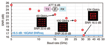
First, we conducted an experiment involving back-to-back data transmission. The TX and RX were directly connected through the attenuator (ATT) with attenuation of 9 dB. The role of this ATT is to protect the RX from the high output power of the PA. The SNR of the received IF signal was measured to evaluate the quality of communication. The SNR is related to the bit error rate (BER). The communication is judged successful when the measured SNR is larger than the required SNR (SNRreq), which is determined as the SNR where the corresponded BER is 10−3 in the following measurement. The SNRreq of 16QAM is 16.5 dB. The measured constellations and dependence of the baud rate with SNR of the received IF signal is shown in Fig. 11. As the frequency utilization efficiency of 16QAM is 4, the data rate is four times the baud rate. In the low baud rate region, the SNR is quite high, more than 25 dB. The SNR gradually degrades with the baud rate because the noise floor also increases with the increase in the baud rate. The maximum baud rate is 31 Gbaud, which corresponds to the very high data rate of 124 Gbit/s.
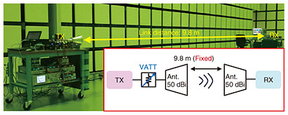
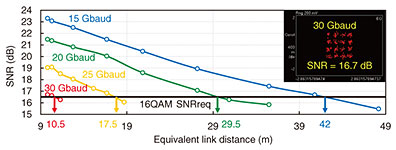
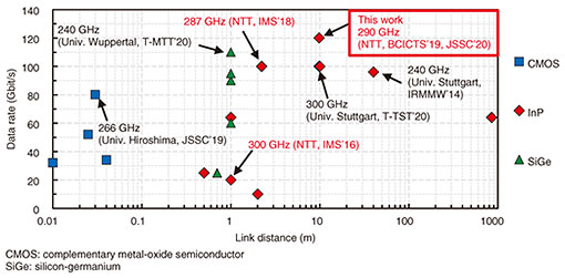
Next, we conducted an experiment involving wireless communication with the TRX with the 50-dBi lensed horn antennas described above. The link distance (TX antenna to RX antenna distance) was fixed to 9.8 m (Fig. 12). However, this link distance was virtually changed by changing the attenuation value of the variable ATT (VATT) inserted between the TX and TX antenna. This VATT equivalently adds the path loss between the TX and RX, and the path loss can be converted to the equivalent link distance. The measured SNR versus equivalent link distances of 15, 20, 25, and 30 Gbaud using the 16QAM signal are shown in Fig. 13. The high data rate of 120 Gbit/s (30 Gbaud) wireless transmission is successfully demonstrated. The received constellation of the 120 Gbit/s IF signal is also shown in Fig. 13. The maximum link distances, which are defined as the equivalent link distance where the SNR is the same as the 16QAM SNRreq, are 42, 29.5, 17.5, and 10.5 m for 15, 20, 25, and 30 Gbaud. The comparison of recently reported near-300 GHz TRX is shown in Fig. 14. The fabricated TRX shows the highest data rate among them.
5. ConclusionWe achieved 300-GHz-band 120-Gbit/s 9.8-m wireless transmission with a 300-GHz-band TRX using the high output power PA fabricated using our in-house InP-HEMT technology. The PA uses a special BDCL to lessen the RF loss and enhance its gain and output power. It achieves a maximum gain of 20.5 dB at 295 GHz, and Psat and OP1dB of 12 and 6 dBm at 296 GHz. The Psat is larger than 10 dBm for 278–302 GHz. The TRX was fabricated using the PA and our in-house 300-GHz fundamental mixer. It achieves a maximum data rate of 124 Gbit/s in 16QAM back-to-back data transmission. Wireless data transmission was successfully demonstrated with a link distance of 9.8 m for data rates of 60, 80, 100, and 120 Gbit/s using 16QAM. To the best our knowledge, the fabricated TRX achieves the highest data rate among the reported 300-GHz-band TRXs. AcknowledgmentsThe authors wish to acknowledge Kenichi Okada of Tokyo Institute of Technology and Ho-Jin Song of NTT Device Technology Labs (now working at Pohang University of Science and Technology) for their fruitful discussions. We also thank the continuous assistant of Yukio Yago at NTT Electronics Techno Corporation. This work was supported in part by the Ministry of Internal Affairs and Communications, Japan, through the Research and Development Program for Expansion of Radio Resources. References
|
||||||||||||||||||||||