|
|||||||||||||||
|
|
|||||||||||||||
       |
Feature Articles: Disaggregated Computing Will Change the World Vol. 19, No. 7, pp. 52–57, July 2021. https://doi.org/10.53829/ntr202107fa7 Disaggregated Computing, the Basis of IOWNAbstractTo achieve IOWN (the Innovative Optical and Wireless Network), we need advanced computer systems that can efficiently process huge amounts of data compared with current capabilities. To meet this demand, NTT is studying an innovative computer architecture, called disaggregated computing, that makes maximum use of photonics-electronics convergence technology. This article describes the overall outline and basic concept of this new computer architecture. Keywords: IOWN (Innovative Optical and Wireless Network), disaggregated computing, photonics-electronics convergence technology
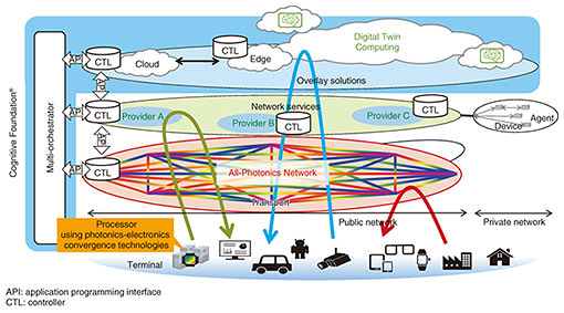
1. IntroductionAlmost everything is connected to networks, and a vast amount of data from them is drastically changing social, economic, and cultural activities. By interconnecting a huge amount of data, it is important to create new value that cannot be obtained only from individual data in such a smart society. To achieve this, not only a broadband network, which transfers data at unprecedented high speed, but also an information processing system with a high processing capacity that is beyond today’s technologies is required. To achieve such a smart society, NTT has proposed the Innovative Optical and Wireless Network (IOWN) [1]. The IOWN Global Forum was founded in 2020 [2] to accelerate innovation of a new communication infrastructure to meet our future data and computing requirements through the development of technologies, frameworks, and specifications. IOWN is a broad vision that includes innovative networks and computing systems boosted by photonics technologies and services provided using them. 2. Computing power for IOWNFigure 1 shows the conceptual diagram of IOWN. It consists of the following elements. The first is the All-Photonics Network (APN), which uses photonics-electronics convergence technology to provide significantly higher bandwidth and lower latency to the network. The second is Digital Twin Computing (DTC) for reproducing the real world in digital space on the basis of a large amount of sensing data from the real world. The third is Cognitive Foundation (CF) for integrated control from the transmission layer to application layer.
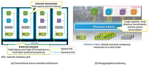
The APN, DTC, and CF require high processing power. In the IOWN era, the network functions implemented by dedicated network nodes, such as routers and mobile base stations, will be implemented as software. Therefore, the network nodes comprising the APN will be computers with high processing power such as high packet-processing rate and huge scheduling capacity. In DTC, computers must process a large amount of data collected from data sources, such as sensors and video cameras, with high definition and granularity. Therefore, they require much higher processing capacity than modern computer systems. CF needs to provide total control and management capabilities for the APN and DTC, such as proper control of computing resources and integrated control of computing resources and networks. To do this, it is necessary to aggregate and analyze a large number of network and computing requests and allocate appropriate bandwidth and wavelength as well as computing resources in a highly real-time manner. This requires quite high processing power that has not been available. Achieving this high processing power with conventional computer architecture requires a large number of servers and consumes significant electric power. To make IOWN a reality, a computer with extremely high performance per unit power is indispensable to obtain the required high processing power without increasing the environmental load. NTT, through three laboratories, i.e., Software Innovation Center, Network Service Systems Laboratories, and Device Technology Laboratories, has begun developing a computer architecture called disaggregated computing, which uses photonics-electronics convergence technology to solve this problem. 3. Details of disaggregated computingFigure 2 shows the concept of disaggregated computing. This new architecture combines a physical configuration (hardware architecture), logical configuration (software architecture), and control scheme to maximize the high-speed, low-power consumption, and low-loss characteristics of photonics technologies and achieve overwhelmingly high performance compared with current computers. This architecture is a paradigm shift from the conventional server-oriented architecture of connecting a closed “computer” in a box via a network to the architecture of directly connecting resources such as central processing units (CPUs) and memory via optical interconnects and treating them as a computer on a rack-scale by using high-speed and long-reach photonics technologies.
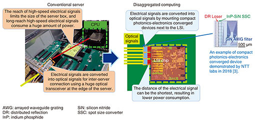
The most important key technology of this architecture is the photonics-electronics convergence technology for enabling large-capacity, long-distance transmission, and low power consumption, which is impossible with electric technology alone. In the conventional server-oriented architecture shown in Fig. 2(a), when data needs to be exchanged between servers, data must be transmitted and received by an external network. As network protocols have evolved to have a deep-layered stack to provide service functions such as reachability and path and session management, the overhead of protocol stack increases to communicate between servers. In disaggregate computing, shown in Fig. 2(b), however, CPUs, graphics processing units (GPUs), field-programmable gate array (FPGAs), and other computing resources are connected via an interconnect (Photonic Fabric) using photonics-electronics convergence technology. This technology eliminates protocol conversion for communication between resources, significantly reducing communication overhead, which is unavoidable in the current architecture. In contrast to the current configuration in which power control and adding hardware resources are done on a per-server basis, disaggregated computing enables power control and adding hardware resources to be done on a per-resource basis, making it possible to provide a more power-efficient and flexible computing environment. The three key points of disaggregated computing are physical configuration, logical configuration, and function-placement control. The following describes each point in detail. 3.1 Point 1: Physical configurationFigure 3 outlines the physical configuration of disaggregated computing. For high-speed electrical signals with speeds over 100 Gbit/s per lane, signal attenuation in the transmission path is a critical issue because of the physical principle that the higher the frequency of an electrical signal, the greater the attenuation in the transmission path. Such a high-speed signal exceeding 100 Gbit/s requires a high-power driver circuit and complex circuit that compensates for the signal waveforms degraded by attenuation. Both consume a huge amount of power. Even if these power-hungry circuits are used, only a few tens of centimeters can be transmitted. On the other hand, optical signals have the advantage of being able to transmit high-speed signals farther than electrical signals, with only 0.2 dB of power loss over 1 km of optical fiber transmission.
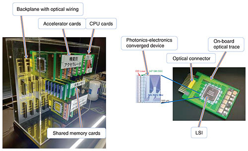
In disaggregated computing, compact photonics-electronics converged devices with high density, wide band, and low power consumption are mounted next to the large-scale integrated circuit (LSI) to immediately convert electrical signals from the LSI into optical signals. Therefore, the distance of the electrical signals can be kept the shortest between the LSI and adjacent photonics-electronics converged devices. By shortening the transmission distance of the high-speed electrical interface from the LSI, the power consumption of the high-speed interface on the LSI can be significantly reduced. NTT Device Technology Laboratories is studying and developing photonics-electronics converged devices for this application, and the details are described in an article in this issue [4]. Figure 4 shows a mock-up of a disaggregated computer. Cards with accelerators, CPUs, and other devices are connected by a backplane with optical wiring. Each card has compact high-density photonics-electronics converged devices mounted next to the LSI. High-speed multi-channel optical signals from the devices are connected to the backplane via optical traces on the card and optical backplane connector.
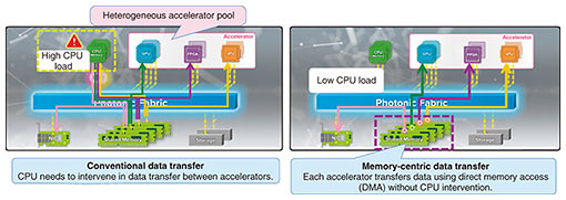
With such a configuration, it is possible to increase the scale of a computer from a box size to a rack-scale, exceeding the limit of the reach of the conventional electric signal. The processing capabilities of the computer can also be increased by adding cards on demand, providing a flexible and efficient system. 3.2 Point 2: Logical configurationFigure 5 shows the logical configuration of disaggregated computing. Although a CPU has the advantage of executing all types of processing, its versatility makes it less power efficient than accelerators for specific workloads.
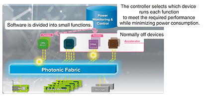
Therefore, with disaggregated computing, we aim to reduce CPU dependency by using accelerators for specific workloads. Accelerators are generally more power-efficient than CPUs when executing specific processes. Since a disaggregated computer using optical interconnect can be made scalable compared with a conventional server, more accelerators can be efficiently aggregated into a computer. This enables a heterogeneous accelerator pool with several different accelerators that can offload the workload on the CPU, improving power efficiency. However, even in this case, if the CPU needs to intervene in data transfer between accelerators, the CPU load will increase and the effect of offloading processing to accelerators will be lost. Therefore, NTT Software Innovation Center is promoting the study of greatly reducing CPU load by memory-centric data transfer without CPU intervention. This accelerator pooling and memory-centric data transfer between accelerators would significantly reduce CPU processing and improve power efficiency, which is described in an article in this issue [5]. 3.3 Point 3: Function-placement controlTo take full advantage of disaggregated computing with physical and logical configurations, it is important to control the arrangement of the software to make the most of this architecture. For this purpose, NTT Network Service Systems Laboratories has proposed power-aware dynamic allocation-control technology for optimum utilization of computing resources, such as CPU and various accelerators, on the basis of software characteristics. As shown in Fig. 6, the software is divided into small functions, and devices such as accelerators and CPUs used by each function are dynamically selected by the power monitor & controller to minimize power consumption. It also uses a normally off device to provide event-driven control that turns on only when necessary. Details are described in an article in this issue [6].
4. Future planNTT laboratories are developing disaggregated computing on the basis of the innovative technologies described above. We will prototype and evaluate trial machines in combination with typical applications, such as image inference, and demonstrate disaggregated computing. In the long term, we will consider the introduction of photonics-electronics convergence technology into LSI chips, the latest research results on optical processing devices, and the development of more advanced architectures. References
|
||||||||||||||