|
|||||||||||||||||||||||||||||||||||||||||||||||
|
|
|||||||||||||||||||||||||||||||||||||||||||||||
       |
Regular Articles Vol. 19, No. 11, pp. 52–58, Nov. 2021. https://doi.org/10.53829/ntr202111ra1 High-gain Optical Parametric Amplifier Module by Using a PPLN Waveguide and Its Application to Quadrature SqueezingAbstractOptical parametric amplification is expected as a key technique for high-speed optical fiber communication and optical quantum computing. We developed a high-gain and broadband optical parametric amplifier (OPA) module by using a periodically poled lithium niobate (PPLN) waveguide, the single-mode core of which is directly bonded to a lithium tantalate substrate. The OPA is assembled as a pump-combiner-integrated module with four optical-fiber input/output ports. By improving the fabrication processes of the PPLN waveguide and the assembly techniques of OPA modules, we achieved over-30-dB phase sensitive amplification with a continuous-wave pump. By using the PPLN waveguide, we successfully obtained over-6-dB squeezed light, the spectral bandwidth of which was 2.5 THz. This high-gain broadband OPA module will help build an advanced information society. Keywords: periodically poled lithium niobate, optical parametric amplifier, squeezed light
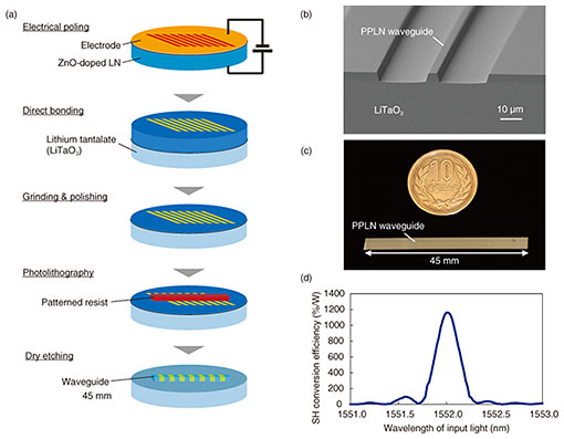
1. IntroductionThe explosive spread of information and communication technologies makes it possible to build an intelligent social and economic system that intricately combines various technologies, such as artificial intelligence and robotics technologies. These information technologies will not only improve our lives but will also promote the sustainable development of the global environment. To ensure this prediction, higher-capacity lower-latency communication and higher-speed lower-power-consumption computation are needed as the technological infrastructure for a future society. However, these techniques are approaching several limits. In optical fiber communication, we are facing limits such as the standard quantum limit for optical linear amplifiers [1] and nonlinear Shannon limit, which determines the practical capacity of optical fiber communication [2]. In the computing field, we are facing the limit of Moore’s law for semiconductor microfabrication [3]. To break these limitations, we conducted research on nonlinear optical devices and their applications to optical fiber communication and optical signal processing. Nonlinear optics describe various nonlinear responses of properties such as frequency and phase of light with strong interaction in nonlinear media [4]. By handling a wide variety of these nonlinear optical phenomena, it is possible to break through the limitations in optical communication and computation mentioned above. For example, by using phase sensitive amplification (PSA) with an optical parametric amplifier (OPA), we can break the standard quantum limit of conventional optical linear amplifiers on the basis of stimulated emission in long-haul fiber communication [5]. Optical phase conjugation by using an OPA can compensate for the nonlinear distortions in optical fibers, which is one factor causing the nonlinear Shannon limit [6]. Wideband optical wavelength conversion also contributes to the expansion of communication resources of wavelengths without reconverting to electrical signals [7]. Regarding computation, OPAs play key roles in non-von Neumann computers, such as a coherent-Ising machine (CIM) [8] and optical quantum computers [9]. In a CIM, an OPA is located in an optical fiber loop and generates artificial spins that have a 0 or π relative phase of light. With the use of time-domain multiplexing and measurement feedforward techniques, the CIM can find solutions for NP (nondeterministic polynomial time)-hard problems such as maximum cut problems. OPAs are also used for quantum light sources for various types of optical quantum computing (QC). For discrete-variable QC, OPAs can generate entangled photon pairs by spontaneous parametric down conversion processes [10]. OPAs also play an important role in continuous-variable (CV) QC because they generate a broadband squeezed vacuum state of light, which is an essential state to generate CV quantum entanglement [11]. Studies have shown the possibility of using OPAs in quantum measurement without electrical circuits [12]. This will be a key technique to achieve ultra-fast QC. With the demand of OPAs for such applications, we developed OPA modules that are based on a periodically poled lithium niobate (PPLN) waveguide [13]. Thanks to its second-ordered nonlinearity, a PPLN waveguide has advantages as an OPA media compared with third-ordered nonlinear media such as high-nonlinear optical fibers. A PPLN-based OPA operates at room temperature without Brillouin scattering under high-power-pump injection, which often becomes a problem with third-ordered nonlinear media, and has the capability of integration in optical circuits. In this article, we introduce our PPLN-waveguide-based OPA module and its application for PSA and optical quadrature squeezing. Our PPLN-waveguide-based OPA module has high pump-power durability, low insertion loss, and high optical parametric gain. The module will be key for future optical communication and computation. 2. PPLN-waveguide-based OPA moduleFor various applications, an OPA should have a fiber-pigtailed configuration with pump combiners. Fiber-pigtailed devices can be used with various reliable optical components, which are sophisticated in optical communication technologies. The configuration promises easy installation into an optical communication system and various quantum technologies for out-of-lab application. 2.1 Waveguide fabricationFor achieving high-gain optical parametric amplification, a PPLN waveguide should have a small core and high durability for a high-power pump and maintain the phase matching condition along it. Figure 1(a) shows the fabrication process of our PPLN waveguide. First, a periodically poled structure is formed by the electrical poling process [14] for an LN wafer. The poling period is about 18 µm. We used a zinc oxide (ZnO)-doped LN wafer because of its high resistance to photorefractive damage [15]. After poling, the wafer was directly bonded to a lithium tantalate wafer. This directly bonded structure also allows us to use high-power light to obtain high nonlinearity [16]. The upper side of the PPLN layer was polished into a thin layer with a thickness of about 5.0 µm. Then, by using photolithography and a dry etching technique, the waveguide structure was obtained. Figure 1(b) shows a cross-sectional view of a fabricated waveguide taken using a scanning electron-beam microscope. To avoid several problems due to the existence of higher-order modes in the waveguide, our waveguide is designed as a single-mode waveguide for light in the communication wavelength band. The waveguide has a length of about 45 mm, as shown in Fig. 1(c). The second-harmonic generation (SHG) efficiency at the phase-matched wavelength is 1200%/W, as shown in Fig. 1(d), which was acquired under 3-mW light injection with a wavelength of 1550 nm. Thanks to the fine processing, the phase matching curve is close to the ideal sinc-squared shape. This means the waveguide’s core has a uniform shape.
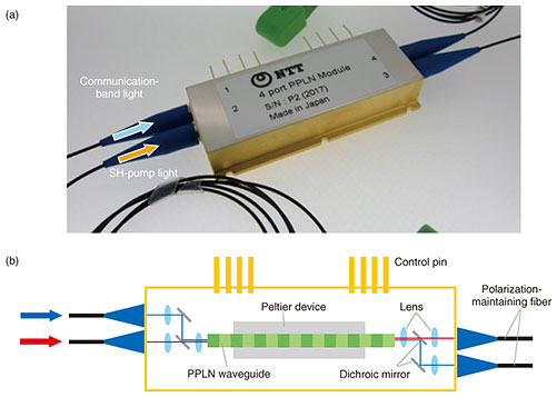
2.2 Module assemblyWe assembled the fabricated PPLN waveguide as a pump-combiner-integrated OPA module with four optical-fiber input/output (I/O) ports [17]. Figure 2(a) shows an overview of the module. The module houses the fabricated PPLN waveguide, six lenses, four dichroic mirrors, and four pigtailed optical fibers, as shown in Fig. 2(b). To suppress optical loss between the waveguide and optical fibers, we designed a spot-size-convertor at both input and output end regions of the waveguide. Thanks to the optimum coupling of both signal and pump lights with the use of two lenses, we obtained coupling losses of 0.5 dB at 1550 nm and 0.7 dB at 775 nm on each side. The total module insertion losses are 2.0 and 2.3 dB for the wavelengths of 1550 and 775 nm, respectively, which include waveguide losses. To maintain the phase-matching condition at any environmental temperature, we placed a Peltier device under the waveguide.
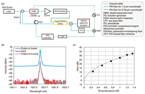
3. ApplicationOur PPLN-waveguide-based OPA module can be used for various applications. In this article, we focus on degenerate PSA for long-haul optical fiber communication and optical quadrature squeezing for CV optical QC. 3.1 Over-30-dB PSAFigure 3(a) shows the experimental setup for degenerate PSA [18]. We used a continuous wave at 1551.6 nm as a signal and pump source. The pump light was amplified using an erbium doped fiber amplifier (EDFA) and launched into a PPLN module for SHG. The generated SH pump was launched into the four-port PPLN module with the signal light to cause optical parametric amplification. The relative phase between the signal and pump was locked using a lead zirconate titanate (PZT)-based fiber stretcher in accordance with the error signal from an optical phase-lock-loop. The output signal light from the PPLN device was detected using an optical spectrum analyzer. Figure 3(b) shows the input and output spectra of degenerate PSA. The difference between the input spectrum and output spectrum without pump corresponds to the insertion loss of 2.0 dB. The input spectrum is amplified with the external gain of 32.3 dB when the injected pump power is 1.35 W. Figure 3(c) shows the external gains as a function of the input pump power. The PSA gains are exponentially increased due to the increase in the SH-pump power without any degradation due to photorefractive damage. This means that our module showed high durability against the high-power SH pump to operate with a continuous-wave-pump power of over 1 W.
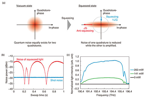
3.2 Optical quadrature squeezingA squeezed vacuum state of light is a non-classical state, which has a reduced quantum uncertainty in a specific amplitude quadrature compared with that of the vacuum state [19], as shown in Fig. 4(a). This state should be used as an essential resource for various optical quantum technologies. For example, by using squeezed light, optical beamsplitters, and optical delay line interferometers, we can generate multipartite optical entanglement, namely an optical cluster state, that is multiplexed in the time domain [20]. This is one of the most important calculation resources in measurement-based QC, which has potential for high-speed large-scale fault-tolerant operation [21]. For achieving this large-scale universal and fault-tolerant QC, a highly squeezed state of light is desired because it results in high-fidelity CV quantum gates and high-dimensional quantum entanglement. For high-speed QC, broadband squeezed light is desired because the maximum clock rate of QC is limited by the bandwidth of the quantum resource. A squeezed light is generated by pumping an OPA and is typically characterized by measuring the variances of the electrical field with balanced homodyne detection [22]. Figure 4(b) shows the measured noise intensities of squeezed light and the vacuum state of light. In accordance with the scanning of the relative phase between the local oscillator and squeezed light, squeezed and anti-squeezed noise are shown one after the other. However, the noise of the vacuum state, namely shot noise, shows a constant value despite the phase scanning. This is because, in the coherent vacuum state, quantum noise equally exists in two optical quadratures. The squeezed level shows over-6-dB noise reduction compared with the vacuum noise. This value exceeds 4.5 dB, which is required for the generation of a two-dimensional optical cluster state. The squeezed light also shows 2.5-THz spectral bandwidth, as shown in Fig. 4(c). This broad bandwidth indicates the possibility of THz-order clock-rate QC. The squeezed light will lead to the development of a high-speed on-chip quantum processor using time-domain multiplexing with a centimeter-order optical delay line.
4. ConclusionWe introduced our broadband high-gain OPA module assembled with a ZnO-doped PPLN waveguide. The PPLN waveguide was fabricated by direct bonding and photolithography. Thanks to the fine process, we can obtain a uniform waveguide and SHG efficiency of 1200%/W. Its directly bonded core enabled us to use over-1-W of pump light to achieve a high-gain optical parametric process without pump-induced degradation. The waveguide is assembled into a pump-combiner-integrated OPA module with four optical-fiber I/O ports. By using this OPA module, we demonstrated over-30-dB PSA even with a continuous-wave pump. This value is sufficient for the amplification gain in long-haul optical communication. We also used the waveguide as an optical quadrature squeezer and obtained over-6-dB squeezed light. This value is sufficient for generating a two-dimensional optical cluster state, which enables multi-qubit computation. The squeezed light also has a 2.5-THz spectral bandwidth. This broad bandwidth indicates the possibility of THz-order clock-rate QC, shortens the length of a flying qumode into sub-millimeter, and enables the implementation of optical delay line interferometers into an integrated optical chip. This broadband high-gain OPA module will break the limits in optical communication and computation. References
|
||||||||||||||||||||||||||||||||||||||||||||||