|
|||||||||
|
|
|||||||||
       |
Feature Articles: The Forefront of Nanomechanics Research Vol. 20, No. 4, pp. 59–64, Apr. 2022. https://doi.org/10.53829/ntr202204fa10 Fabrication of Suspended Nanowire Mechanical Devices Using Inkjet TechnologyAbstractSemiconductor nanowires are attracting attention as building blocks for next-generation electrical and optical devices. When nanowires are suspended, they function as nanomechanical devices with specific mechanical properties, thus are expected to be applied to high-sensitivity sensors. This article explains how such a nanomechanical device can be easily and efficiently fabricated using inkjet technology while minimizing resource waste. Keywords: nanowire, inkjet, nanomechanical device
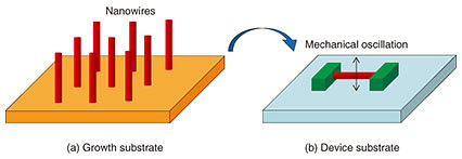
1. Inkjet printersInkjet printers are common household electrical appliances used for printing from personal computers to paper. They are also used in various industrial fields to, for example, print characters on three-dimensional objects, such as dates on plastic bottle caps. Such three-dimensional printing is possible because the printer head does not directly contact the object on which characters or pictures are to be printed. There are two main types of ink-ejection methods for conventional inkjet printers. One is the piezo method, which pushes out ink by pressure, and the other is the thermal method, which pushes out ink by heating. The minimum size of a droplet ejected from a home inkjet printer is approximately 1 pL, and the diameter of a droplet moving through the air is said to be approximately 10 µm. However, the actual minimum printing resolution is several tens of micrometers, because the droplet spreads slightly from the time it reaches a printing object such as paper until it dries. Inkjet printers can not only print characters and pictures on paper but can also directly “print” electronic circuits just like those on printed circuit boards. Because the inkjet printers can arrange materials such as metal electrodes without a photomask and do so on demand, thus, it can be applied to microstructure formation on soft organic materials that are incompatible with conventional top-down methods such as photolithography. The inkjet method can also be applied to flexible electronic devices that can be attached to living tissue such as human skin. When a metal pattern is formed using the conventional lift-off method, a large amount of material is wasted because only part of the deposited metal is left on the substrate as electrodes and wiring; the majority is removed together with the photoresist. However, with the inkjet method, only the necessary amount of material can be placed on demand at the desired location. This is advantageous from the viewpoint of saving resources. 2. Nanomechanical device using semiconductor nanowireOur research group has mainly studied mechanical devices on the micrometer scale. We focus on semiconductor nanowires as mechanical vibration elements with a cross-sectional size on the nanometer scale. As schematically shown in Fig. 1(a), nanowires are whisker-shaped crystals that are grown at an angle along a certain crystallographic orientation with respect to a semiconductor substrate. They are typically a few hundred nanometers in diameter and about ten micrometers in length. Although nanowires as grown on the substrate can be processed into devices such as lasers and transistors (vertical devices), we decided to transfer nanowires to another device substrate, as shown in Fig. 1(b), to fabricate a horizontal doubly clamped beam structure for better control of the mechanical properties. We use indium arsenide (InAs) as the semiconductor material because electrons accumulate on the surface and good electrical contact can be obtained.
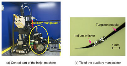
The most primitive means of transferring nanowires from a growth substrate to another substrate for fabricating nanomechanical devices is to rub a piece of the growth substrate against the device substrate or take up some nanowires on a cotton swab and press them on the device substrate. With this method, however, the positions where the nanowires are transferred on the device substrate are determined entirely by chance. If we retrofit the electrodes to the location of the nanowire, we may find a nanowire that can be used somewhere on the device substrate. However, we cannot rely on chance because we need to suspend the nanowire over a pre-patterned groove, as explained later. Even if a nanowire is accidentally transferred to the desired position, most of the other nanowires are not used and are wasted. To avoid such inefficiency and waste, it is necessary to place the nanowires at predetermined positions on the device substrate while observing them in real time with an optical microscope. A resin film, such as electron-beam resist, is often used to pick up small pieces of thin films, such as graphene, and transfer them to another substrate. Although this technique can be applied to nanowire transfer, we developed a method using an inkjet printer for more efficient transfer. We used a high-specification machine dedicated for research purposes that can eject ultrafine droplets that are about 1/1000 the size of droplets from household inkjet printers [1]. The discharge method is an electrostatic one that differs from the two common methods described above. Although the machine is larger than a household inkjet printer, it is still desktop size and can be operated relatively easily under normal temperature and pressure. 3. Fabrication of nanowire mechanical device by using inkjet methodFigure 2(a) shows a photograph of the main part of the actual inkjet machine (manufactured by SIJTechnology). The inkjet nozzle is located under the red cylindrical part that can be seen at the back of the observation camera, enabling precise control along the X, Y, and Z axes. We added our developed auxiliary manipulator. As shown in the enlarged photograph in Fig. 2(b), a thin whisker of indium (a few micrometers in tip diameter) is attached to the tip of a tungsten needle and used to finely adjust the position of the nanowires once they have been inkjetted onto the device substrate [2].
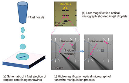
In actual transfer operations, nanowires are dispersed in a slow-evaporating solution called butylcarbitol, which is then filled into an inkjet machine as “ink.” A sufficient number of nanowires can be dispersed by brushing off nanowires from a small area of a few millimeters in the growth substrate with a thin brush. Figure 3 shows a schematic diagram of the process of ejecting droplets of butylcarbitol solution containing nanowires as well as optical microscope photographs taken during an actual transfer operation. As shown in Fig. 3(b), butylcarbitol droplets are ejected into several areas that appear as black ellipses in a low-magnification optical micrograph viewed from an oblique direction. To transfer nanowires with a length of about 10 µm, a nozzle with a relatively large diameter is used. Therefore, considerably large droplets for this inkjet machine (a little less than 50 µm in diameter) are ejected. As shown in the high-magnification optical micrograph in Fig. 3(c), two sets of right and left microelectrodes are formed beforehand on a silicon (Si) substrate, and droplets are ejected aiming at each electrode group. The evaporation of butylcarbitol progresses, and the droplets almost disappear, but the nanowires are not completely fixed to the substrate yet. From the photo on the left in Fig. 3(c), the concentration of the nanowire dispersion is adjusted so that each droplet contains one nanowire, but the nanowire does not yet sit on the electrodes due to the large original droplet size. The position of the nanowires is then adjusted with the auxiliary manipulator of whiskered indium, as shown in the right photo of Fig. 3(c), where each nanowire is found on top of and perpendicular to the electrodes. At this time, the nanowire is moved together with each droplet, or a solution is left between the nanowire and the substrate, so that no excessive force is applied to the nanowire. Even if the tip of the manipulator directly touches the nanowire, it will not damage the nanowire because indium is soft metal. By using the auxiliary manipulator in this manner, the nanowire can be finally positioned with an accuracy of about 1 µm.
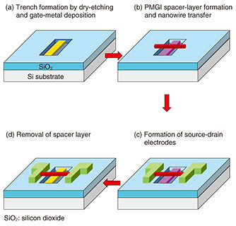
Figure 4 shows the flow for fabricating a nanomechanical device. First, a trench is dry-etched into a surface oxide layer on a Si substrate, and back-gate metal for electromechanical control is deposited in the trench. The final difference between the trench depth and gate-metal thickness is the distance between the nanowire and gate (approximately 300 nm). If the nanowire is transferred directly above the gate metal with an air gap, it will be pulled down and come into contact with the gate surface in the lift-off process, preventing free mechanical motion. Therefore, the trench is first covered with a resin spacer layer called polydimethylglutarimide (PMGI), onto which the nanowire is transferred using the inkjet method. After the source/drain electrodes for electrical measurement have been formed by lithography and lift-off, the spacer layer is removed by isotropic ozone cleaning in the gas phase, and the fabrication of a suspended nanomechanical device is completed.
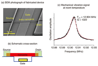
A scanning electron microscope (SEM) photograph of the fabricated nanomechanical device and schematic cross-sectional view are shown in Figs. 5(a) and (b), respectively. The length of the vibrating segment of the nanowire is 10 μm, and the width of the back gate, which is electrostatically coupled to the nanowire via a 300-nm gap, is 4 μm. As shown in Fig. 5(c), the signal from the mechanical vibration was detected by monitoring the current flowing between the source and drain electrodes while applying a high-frequency voltage to the gate electrode, which exerts an alternating electrostatic force on the nanowire. A Lorentzian-type resonance peak was observed at around 12.9 MHz, which is close to the resonance frequency calculated from the length and diameter of the nanowire, indicating that a suspended nanomechanical device was properly fabricated [3].
4. Future developmentsThe typical size of a semiconductor nanowire, 100 nm in diameter and 10 µm in length, is close to the minimum size that can be manipulated while observing it in real time with an optical microscope at room temperature and atmospheric pressure. Although the inkjet printer uses micrometer-scale technology, the gap between a micrometer-scale system and nanometer-scale one can be bridged via nanowires with submicrometer diameters. As a result, applications can be expanded to regions with a higher resonance frequency and high-sensitivity sensors that can detect single molecules adsorbed on nanowires by reducing the mass of the beam structure. References
|
||||||||