|
|||||||||||||||
|
|
|||||||||||||||
       |
Feature Articles: Plasmon Control Technology Vol. 21, No. 5, pp. 34–39, May 2023. https://doi.org/10.53829/ntr202305fa5 Time-resolved Measurement of Ambipolar Plasmon Transport in Semiconductor Composite Quantum WellsAbstractTwo-dimensional topological insulators have attracted much attention for potential application to quantum computers on the basis of a new principle. Semiconductor composite quantum wells, in which electrons and holes are confined in separate layers, can serve as two-dimensional topological insulators when their layer structure is optimized. We describe time-resolved measurements of ambipolar plasmon transport in both the electron and hole regimes separately using a single device. This technique will pave the way for investigations of charge and spin dynamics in two-dimensional topological insulators. Keywords: two-dimensional topological insulators, topological quantum computing, plasmonics
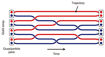
1. Topological quantum computingNext-generation computers based on new operating principles have been attracting much attention for solving problems such as combinatorial optimization problems, which are difficult to achieve with conventional computers. Quantum computers that execute massively parallel computation by simultaneously encoding multiple units of information on the basis of the principles of quantum mechanics have been extensively investigated. Various proof-of-principle experiments, including fundamental quantum operations such as quantum entanglement, have been demonstrated using single atoms, photons, and electron spins to implement qubits for practical applications. For social implementations of quantum computers, fault-tolerant quantum computation and scalable quantum circuits are recognized as key issues. Topological quantum computation with quasiparticles,*1 the unique properties of which differ from those of natural elementary particles,*2 has been proposed as an alternative approach. Differently from conventional quantum computing, topological quantum computation uses changes in the quantum state of the system triggered by the exchange of quasiparticles as a logic gate. Calculations are executed by sequentially exchanging quasiparticles arranged in space (Fig. 1). Since the result is determined only by the order in which the quasiparticles are exchanged and does not depend on the details of the trajectory of the quasiparticles, this qubit is expected to be fault-tolerant against external noise. The two-dimensional topological insulator is expected to serve as a platform on which quasiparticles with unique properties can be generated.
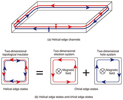
2. Two-dimensional topological insulatorIn two-dimensional topological insulators, the interior of the sample is insulating while one-dimensional conductive channels with opposite spins propagating in opposite directions (helical edge channels) are formed along the edge of the sample (Fig. 2(a)). Since inelastic scattering between the channels is prevented by time-reversal symmetry,*3 backscattering is suppressed at zero magnetic field if the sample has no magnetic impurities. The quasiparticles that are key ingredients for a topological quantum computing (Majorana quasiparticles) are expected to appear in systems where a superconductor is brought to close proximity with the helical edge states. The conductance of the helical edge states should be quantized as theoretically predicted. In experiments, however, quantized conductance*4 has been observed only in samples that have a scale of several micrometers, and the details of the dissipative transport mechanism have not been experimentally understood. When a strong magnetic field is applied to a two-dimensional electron (hole) system, the cyclotron motion of electrons (holes) is quantized, forming discrete energy levels called Landau levels. In this case, if the Fermi level is placed between the Landau levels, the interior of the sample becomes insulating and one-dimensional conductive channels for which the propagating direction is determined by the magnetic-field direction and charge-carrier type are formed along the edge of the sample (chiral edge channels). This phenomenon is called as a quantum Hall effect, and the system is classified as a two-dimensional topological insulator with broken time-reversal symmetry. Helical edge states in a two-dimensional topological insulator with time-reversal symmetry can be approximately thought of as a superposition of chiral edge states of electrons and holes moving in opposite directions, ignoring the exact spin orientation (Fig. 2(b)). At NTT Basic Research Laboratories, we therefore focused on edge transport of plasmons (edge magnetoplasmons) in indium arsenide/indium gallium antimonide (InAs/InGaSb) composite quantum wells, the base material of semiconductor two-dimensional topological insulators. Edge magnetoplasmons are collective oscillations of charges at the edges of two-dimensional systems. By investigating their dissipation and propagation velocity, we can evaluate the characteristics of the edge states.
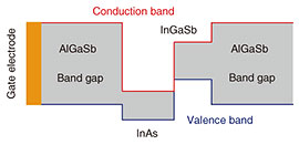
3. InAs/InGaSb composite quantum wellA composite quantum well consists of InAs and InGaSb sandwiched between aluminum gallium antimonide (AlGaSb) barrier layers. Figure 3 shows the energy band diagram, where electrons and holes are confined in the InAs and InGaSb quantum wells, respectively. When the bottom of the InAs conduction band is lower than the top of the InGaSb valence band (band-inversion), hybridization of the electron and hole states opens an energy gap, resulting in a two-dimensional topological insulator [1]. When the bottom of the InAs conduction band is higher than the top of the InGaSb valence band (non-band-inversion), the semiconductor has a normal band gap. However, the charge-carrier type can be switched between two-dimensional electron and hole systems by controlling the Fermi level with a voltage applied to the surface gate electrode. We carried out on-chip time-resolved measurements of edge magnetoplasmons in both two-dimensional electron and hole systems using non-band-inverted composite quantum wells.
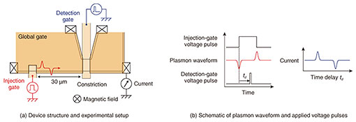
4. Time-resolved transport-measurement schemeConventionally, time- or frequency-domain transport of plasmons in the gigahertz range has been measured with a sampling oscilloscope or spectrum analyzer. However, it has been difficult to observe and evaluate the original plasmon waveform inside a sample because of measurement sensitivity and distortion of high-frequency signals in the measurement system. We succeeded in observing edge magnetoplasmon waveforms inside samples in the time domain by using a method that is similar to pump-and-probe spectroscopy in optical measurement. Figure 4(a) schematically shows the device structure and experimental setup used in the time-resolved measurements. The structure has an injection gate for exciting edge magnetoplasmons, detection gate for the time-resolved measurement, and global gate for controlling the charge-carrier types and densities. These gates are insulated from each other and from the semiconductor substrate by aluminum oxide (Al2O3) insulating layers so that gate voltage can be applied independently to each gate electrode. In addition to an Ohmic contact for measuring current, there are several Ohmic contacts for stabilizing the device under the applied high-frequency voltages. The measurements were carried out in the quantum Hall regime under a strong magnetic field at a measurement temperature of 1.5 K. When a voltage pulse is applied to the injection gate (injection pulse), negative and positive pulsed edge magnetoplasmons are excited at the rising and falling edges of the injection pulse, respectively. The excited edge magnetoplasmons propagate along the edge of the device to the right or left, depending on the chirality determined by the magnetic-field direction and charge-carrier type. For the time-resolved measurement, a short voltage pulse (detection pulse; about 80 ps in width) is applied to the detection gate, which is 30 μm from the injection gate, to temporarily modulate the local carrier density in a constriction (Fig. 4(a)). If the detection pulse coincides with the arrival of edge magnetoplasmons on the constriction, the edge magnetoplasmons are reflected at the constriction; otherwise, the edge magnetoplasmons are transmitted through the constriction and measured at the Ohmic contact located to the right of the constriction. The waveform of the local edge magnetoplasmons propagating in the device can thus be obtained by measuring the current as a function of the time delay td on the detection pulse from the injection pulse (Fig. 4(b)) [2].
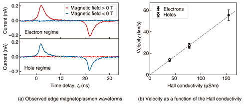
5. Time-resolved measurement of edge magnetoplasmonsAn example of edge magnetoplasmon waveforms measured in the electron and hole regimes are shown in Fig. 5(a), where the origin of the time axis represents the time of edge magnetoplasmon excitation. The timing of the positive and negative pulsed waveforms corresponds to edge magnetoplasmons excited at the rising and falling edges of the injection pulse, and the time interval corresponds to the width of the injection pulse. Pulsed waveforms are observed for only one magnetic-field direction depending on the charge-carrier type since electrons and holes have opposite chiralities in the same magnetic-field direction. The peak delay of about 2 ns, which corresponds to the propagation time of the edge magnetoplasmons on the propagation distance (30 μm) yields the propagation velocity. Theoretically, the propagation velocity of edge magnetoplasmons is proportional to the Hall conductivity when the surface of the device is covered with a metallic gate electrode. The measured propagation velocities for edge magnetoplasmons in the electron and hole regimes are almost identical and proportional to the Hall conductivity (Fig. 5(b)). Therefore, the propagation of edge magnetoplasmons in both the electron and hole regimes can be measured in the time domain. This result indicates that the characteristics of the edge channels can be measured as the propagation velocity of the edge magnetoplasmons.
6. Future prospectsAt NTT Basic Research Laboratories, we observed edge magnetoplasmon waveforms in the time domain in both electron and hole regimes of an InAs/InGaSb composite quantum well, which is the base material of a two-dimensional topological insulator. Since the measured propagation velocity of edge magnetoplasmons reflects the properties of the edge channels, this time-resolved measurement scheme can be used to investigate charge and spin dynamics and its relaxation mechanism on various materials, including two-dimensional topological insulators. Such experiments will pave the way for developments in topological quantum computing. Furthermore, control of the propagation velocity and chirality of edge magnetoplasmons with gate voltage and magnetic fields are expected to be powerful techniques for plasmonics, in which plasmons are used as information carriers. References
|
||||||||||||||