|
|||||||||
|
|
|||||||||
       |
Front-line Researchers Vol. 21, No. 5, pp. 6–11, May 2023. https://doi.org/10.53829/ntr202305fr1  Researchers Have a Responsibility to Create New Knowledge and Technology and Let That Responsibility Be RewardingAbstractNTT Nanophotonics Center is investigating photonics-electronics convergence technologies with the aim of creating low-latency and low-energy-consumption optical computing technology. As various types of photonic information processing are becoming possible, Masaya Notomi, a senior distinguished researcher at NTT Basic Research Laboratories and project leader of NTT Nanophotonics Center, is pursuing the control of optical properties of materials and device applications by using artificial nanostructures. We interviewed him about the progress of his research activities and his attitude as a researcher. Keywords: nanophotonics, photonics-electronics convergence, topological photonics
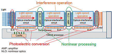
Pursuing new phenomena and photonic processing devices by using integrated nanophotonics—Our last interview was in 2020. Can you tell us about the progress of the research you are conducting? Since joining NTT, I have been pursuing the discovery of new phenomena and development of photonic processing devices using integrated nanophotonics. More specifically, I have been engaged in creating new nanophotonics structures by using state-of-the-art nano/microfabrication techniques, discovering new physical phenomena manifested in those structures, and developing technologies to fabricate photonics-electronics convergence information-processing chips with ultrahigh speed and ultralow energy consumption. Modern photonics technology is the driving force behind high-capacity information transmission such as long-distance optical-fiber communications and server-to-server communications within datacenters. Research is trending toward applying the high-speed and large-capacity properties of light to the circuits inside devices, and the ultimate form of the application of light is the configuration of optical network circuits in computer chips and direct information processing using light. Although the creation of an optical computer has long been one of the major goals of researchers in the field of optics, in a world where complementary metal-oxide semiconductor (CMOS) electronic circuit technology is gaining prominence, the significance of using light for arithmetic processing has not been recognized in terms of ease of implementation and cost. As the limits of miniaturization and integration of CMOS technology (the so-called “end of Moore’s law”) gradually approach, expectations for arithmetic processing taking advantage of the high-speed nature of light are growing. Integrated nanophotonics technology makes it possible to achieve such processing. With nanophotonics technology, highly advanced semiconductor nano/microfabrication techniques are used to create nanometer-scale structures that are the same size as (or smaller than) the wavelength of light, which enables miniaturization of devices and creation of new optical properties that would be unfeasible with conventional optical devices. An example result of the application of nanophotonics technology is a photonic crystal, which is an artificial structure in which refractive index is periodically modulated on a submicron scale. We have used this crystal to fabricate ultrasmall devices and devices with ultralow energy consumption. Although optical arithmetic processing is anticipated, it is currently difficult to execute various general-purpose processing operations on optical circuits only. Therefore, we focused on combining the complex digital signal processing and large-capacity memory of electronic circuit technology with optical circuit technology that carries out the processing that light excels at to accelerate specific arithmetic processing operations, namely, functionalization of the optical circuit as an accelerator. In addition to digital signal processing, analog signal processing plays an important role in machine learning, which is increasingly in demand, and the value of using light in analog signal processing is being recognized. We have therefore set a goal of creating a photonics-electronics convergence accelerator that combines CMOS electronics and nanophotonics, as shown in Fig. 1. This accelerator will enable (i) light-speed operations exploiting optical propagation (especially optical interference), (ii) improvement in the efficiency of photoelectric conversion and digital-to-analog conversion through the fusion of photonics and electronics at the arithmetic processing level, and (iii) generation of effective nonlinear optical properties by using optical transistor technology.
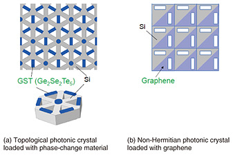
—You are involved in research with high academic and social expectations, right? Under the title of “Development of a photonics-electronics convergence computing infrastructure utilizing spatial, temporal, and wavelength degrees of freedom,” our research on developing a low-latency and low-energy-consumption computing accelerator was selected as a research project of the Japan Science and Technology Agency’s Core Research for Evolutionary Science and Technology (JST-CREST) in 2021 in conjunction with the National Institute of Advanced Industrial Science and Technology (AIST), Nagoya University, Kyoto University, and Kyushu University. In this research project, we are pursuing photonics-electronics convergence information processing, which combines transmission using optical technology with CMOS technology to enable high-speed signal processing that takes advantage of the properties of light. On the basis of the photonics-electronics convergence technology to be implemented around 2030, which is the commercialization target of the Innovative Optical and Wireless Network (IOWN), we are considering the application of this information processing to a computer system that uses optical signals for certain information-processing operations in the chip. Two key points must be addressed in this research project. The first is to solve the problem regarding the integration of CMOS circuits and optical circuits. The key to this integration is to create high-density optical-electronic interfaces by reducing the size and energy consumption of electrical-to-optical converters (EO conversion), such as optical modulators, and optical-to-electrical converters (OE conversion), such as photodetectors. We have built the world’s first femtofarad-level-capacitance photoelectric conversion device using photonic-crystal technology and demonstrated that by suppressing capacitance, photoelectric conversion is possible with very little energy consumption. I believe that this technology will enable the first photonics-electronics convergence computing system that seamlessly fuses light and electricity to achieve both high computing power and low power consumption. Another important aspect of this highly efficient photoelectric conversion technology is the ability to add new functions to light. By using integrated nanophotonics technology, we developed a nanophotodetector-nanomodulator integrated device (OEO-conversion device), a photonics-electronics-converged device with both OE conversion and EO conversion functions and is very small (10×15 µm2). We have succeeded in operating this device as an optical transistor. Since optical transistors can execute nonlinear processing, which has conventionally been difficult with light, we believe this device can be used for nonlinear processing, as shown in Fig. 1, and be a key device in photonics-electronics convergence neural-network (NN) processing. A critical step toward ultralow-latency and low-energy-consumption information processing systems—You are achieving fantastic results. Would you tell us about the second key point in the research project? The second key point is arithmetic operations using optical interference. Optical interference enables operations to be executed at the speed of light. We proposed an optical parallel adder as an application of binary-decision-diagram (BDD)-based digital arithmetic. This arithmetic unit executes digital addition through a single photoelectric conversion and optical propagation and is expected to achieve a latency about one order of magnitude lower than that of CMOS adders. In cooperation with a research group of AIST, we fabricated a prototype of a 4-bit optical adder and successfully demonstrated full additive operations. Regarding the BDD-based digital arithmetic, we found that circuit size increases exponentially by using multipliers, etc. and searched for a means to avoid this problem. We discovered that circuit size can be reduced using the above-mentioned optical transistors at key points. Optical interference is an analog operation, so light is most advantageous in analog operations. A typical example of an analog operation that can be executed at the speed of light is a multiply-accumulate operation, which is the most-fundamental operation and a processing bottleneck in deep learning and artificial-intelligence processing using modern NNs. Therefore, we are investigating a photonics-electronics convergence NN architecture using multiply-accumulate operations exploiting optical interference. We plan to execute a multiply-accumulate operation with an optical circuit using optical interference and execute nonlinear processing called activation, which is necessary at key points in NN processing, with an optical transistor. We then envision a scenario in which we integrate this high-speed analog computing circuitry using light with a CMOS processor by using highly efficient photoelectric conversion technology. In this scenario, the conversion of electrical digital signals to optical analog signals is important. We discovered that digital-to-analog conversion with ultralow latency is possible with the above-mentioned linear-interference logic gate technology and successfully demonstrated circuit operation in collaboration with AIST. To develop component technologies in accordance with the above-mentioned scenario, NTT and AIST developed a prototype optical circuit using advanced silicon-photonics integration technology and are verifying the principle on which the prototype is based. At the same time, a research group at Kyushu University, which has expertise in computer architecture, has been studying an architecture for a photonics-electronics convergence computing system having scalability for large-scale operations achieved by integrating the above-mentioned multiply-accumulate operation unit with CMOS arithmetic circuits. This research project aims to develop a photonics-electronics convergence accelerator that can operate cooperatively with CMOS by making the most of the characteristics of light-speed operation. We expect that this development will be an important step toward implementing an ultralow-latency and low-energy-consumption information-processing system that is required in the post-Moore era. —I heard that you have achieved new results concerning topological photonics, which you talked about in the previous interview. As I reported in the previous interview, we are also conducting basic research to discover new properties of light; in particular, we are working on a new field called topological photonics. This field involves the creation of new physical properties of light by applying the concept of topology to photonic crystals, which we have been researching for many years, and is currently the subject of research activities worldwide. We are particularly focused on developing a dynamically reconfigurable optical-topology system. In topological photonics, new properties are constantly being discovered, and if we can dynamically control these properties, we expect to be able to achieve operations that are currently impossible with conventional optical devices and circuits. We aim to propose two methods for controlling light through optical topological phase transition and dynamic change in optical topology: (i) loading and modifying a nanophotonic structure with functional nanomaterials and (ii) using the peculiar properties of non-Hermitian optical periodic systems using the imaginary part of the refractive index*1. Regarding the technology for controlling a nanophotonics structure by adding nanomaterials, we are investigating a method of loading a photonic crystal with a phase-change material, the optical properties of which change significantly with temperature and other factors. By patterning germanium-antimony-telluride (GST)*2, an excellent phase-change material, and loading it on a photonic crystal, as shown in Fig. 2(a), we found through theoretical analysis that it is possible to induce an optical topological phase transition through a phase change of GST. To demonstrate this theoretical phenomenon, we developed technology for fabricating nanostructures using film deposition and high-precision alignment techniques and succeeded in fabricating silicon topological photonic-crystal structures loaded with submicron-scale GST. We are currently attempting to induce an optical topological phase transition through the crystalline amorphous phase transition of GST. Thus far, we have developed a laser using an ultracompact current-injection photonic crystal nanoresonator. Using this laser, we recently fabricated—as a world’s first—a coupled system in which two nanolasers are integrated, and used this system to generate a special light state called an exceptional point peculiar to non-Hermitian optics. We also succeeded in observing direct emission of light from this exceptional point. We proposed a method for fabricating a new type of photonic crystal called a non-Hermitian photonic crystal, in which the imaginary part of the refractive index is periodically modulated. As shown in Fig. 2(b), this fabrication process involves patterning graphene*3 loaded on a photonic crystal with submicron periodicity. We clarified that an exceptional point can be formed on this structure.
We are currently conducting experiments related to generating optical topological-phase transitions and forming topological singularities, which have been initially observed, to obtain quantitative data. For non-Hermitian photonic crystals, we fabricated devices that can control the imaginary part of the refractive index using a technique for selectively loading graphene and researching the control of exceptional points and topological singularities. Although research on topological photonics and non-Hermitian optics is still in the exploratory basic-research stage, a variety of unknown properties that differ from those of conventional materials have been discovered, and exciting research and development is being conducted worldwide. Singularities with peculiar properties, such as exceptional points and topological singularities, have been reported, and we are conducting our research with the expectation that we will find new means of optical control that will use those properties.
Having light execute computation—I understand that your research on optical transistors was the impetus for the IOWN concept. I am glad that our research on photoelectric conversion and optical transistors based on nanophotonics was one of the triggers that hatched the IOWN concept, which aims to introduce light into all areas of communication networks. That said, it was a happy accident. I am quite interested in having light execute computation (in addition to communication), and I believe that light can do a lot more. This idea may sound a bit far-fetched, but in the brain, computations are executed as a result of signals propagating through the NN in the brain. I thought that light, rather than electricity, was more appropriate for those computations. Computing with optical networks can be much faster, so things that were previously unimaginable become possible. In other words, I hope that the pursuit of having light execute computation will lead to the technological elements that will form the foundation of IOWN. Realizing this idea of having light execute computation through the development of an optical integrated circuit was up for internal discussion during our research on photonic crystals, but we thought it would be a difficult target to achieve. In fact, our collaboration with experts in computer science at JST-CREST led to the actual consideration of the idea. As we began to work with experts in completely different fields, what had previously been a vague idea became a concrete research topic. Through that experience, I realized—even more strongly—that it is important to look at other fields and other worlds. —What do you think researchers are to society? And what would you like to say to future generations of researchers? It is our responsibility as researchers to create new knowledge and technologies, and I believe that such a responsibility can be rewarding. If there are no more researchers, current technologies will be unusable or not even exist. In that sense, researchers are necessary for society and to move it forward. To have my responsibility be rewarding, I try to ensure enough time for my research. Routine tasks come up constantly, but I allocate my time wisely. I think it is important to set aside half a day, or even a full day, for me to concentrate and think freely without being overwhelmed by routine tasks. Having said that, I’m currently in a difficult situation as a researcher because I do not have enough time to spare. If I become aware that I’m in such a situation, I try to find such time, even if I have to push myself. Finally, to all researchers, remember when you first joined a lab at university and the feeling you had when you were conducting experiments and research for the first time. The research and experiments must have been exciting, right? Today’s researchers are really busy every day, and I think it is easy to forget what we were like back then, but let’s not forget the fun of pursuit and create that fun by ourselves. Exciting research requires preparation. I want you to conduct research in a manner that enables you to continue with that fun. To students who aspire to become researchers, I feel that Japan today has too few students going on to doctoral programs. In Europe and the United States, a doctoral degree is recognized as a status not only for researchers but also for engineers. Therefore, if you aim to become a researcher or engineer who can play an active role in the world, you should obtain a doctoral degree. When you decide what you want to be/do in the future, don’t look at society from a short-sighted perspective but from a long-term perspective. ■Interviewee profileMasaya Notomi received a B.E., M.E., and Ph.D. in applied physics from the University of Tokyo in 1986, 1988, and 1997. In 1988, he joined NTT. Since then, his research interest has been to control the optical properties of materials/devices by artificial nanostructures (quantum wires/dots and photonic crystals). He is also a professor at Tokyo Institute of Technology. He received the IEEE Laser and Electro-Optics Society Distinguished Lecturer Award in 2006, JSPS prize in 2009, Japan Academy Medal in 2009, and the Commendation by Japanese Minister of Education, Culture, Sports, Science and Technology in 2010. He served as a member of the National University Corporation Evaluation Committee in the Japanese government. He is an IEEE Fellow and member of the Japanese Society of Applied Physics, American Physical Society, and Optica. |
||||||||