|
|||||||||
|
|
|||||||||
       |
Front-line Researchers Vol. 21, No. 8, pp. 6–10, Aug. 2023. https://doi.org/10.53829/ntr202308fr1  Aiming to Become a Visible Researcher by Taking Up Challenges without Fear of FailureAbstractGreen innovation involves creating new solutions to environmental problems and sustainable development, and research and development of innovative technologies in the fields of the environment, resources, and energy is being conducted worldwide to create a low-carbon and circular society. We interviewed Yoshitaka Taniyasu, a senior distinguished researcher at NTT Basic Research Laboratories, who has produced world-class research results concerning functional materials for green innovation, about his achievements and attitude as a researcher. Keywords: materials research, green innovation, aluminum nitride
Pursuing functional materials for green innovation and solving social problems—Could you tell us about the research you are currently conducting? I’m currently researching functional materials for green innovation. When I was appointed as a senior distinguished researcher, I chose green innovation as a research theme that I would pursue for the long term. As you know, reducing carbon dioxide is a global challenge. Addressing growing demands for efficient use of energy, effective utilization of limited resources, and creation of a sustainable society, researchers like me are taking up the challenge through approaches such as developing methods to generate energy and use energy efficiently. As a researcher specializing in materials research, I’m researching and developing technologies for synthesizing and controlling the properties of next-generation materials to fabricate new functional devices that contribute to the creation of a sustainable society. My specific objectives are to (i) elucidate the physical properties of materials, (ii) make devices more efficient with lower loss on the basis of scientific principles, and (iii) demonstrate the principles of device operation by establishing technologies for synthesizing new materials and fabricating devices using those materials. The discovery and synthesis of new materials and innovations in device technology can significantly change society, and this potential is what makes materials research so interesting. In 2002, my colleagues and I were the first in the world to demonstrate the use of aluminum nitride (AlN), which had been used as an insulator since its synthesis more than a century ago, as a semiconductor. That breakthrough opened up the possibility of applying AlN to semiconductor devices. In this interview, I will talk about our impactful research results concerning AlN that will contribute to green innovation. —Research results that will contribute to solving social problems and have an impact on the world sound very exciting. In 2006, for the first time in the world, we succeeded in operating a light-emitting diode (LED) based on AlN, which is theoretically predicted to emit light with the shortest wavelength among all semiconductors. We observed light in the deep ultraviolet (UV) region (210-nm wavelength) from the AlN LED. AlN is a direct-bandgap semiconductor and has the same crystal structure as gallium nitride (GaN), which is widely used in blue LEDs and semiconductor lasers for high-density digital versatile discs. AlN has the largest bandgap energy (i.e., the energy required for an immobile electron to become a free electron) among semiconductors, i.e., 6 eV. Accordingly, it is theoretically predicted that if AlN LEDs could be fabricated, they would emit light at a wavelength of 210 nm, which is the shortest among all semiconductors. In the UV spectrum, light with wavelength in the range of 300 to 400 nm is called “near UV,” and light with wavelength in the range of 200 to 300 nm is called “deep UV.” In addition, UV light with a wavelength of 200 nm or less, known as “vacuum UV,” is absorbed by the atmosphere and can only be used in a special environment such as a vacuum. Widely used deep-UV light sources are gas-light sources such as mercury lamps and gas lasers. However, mercury lamps use hazardous substances, and gas lasers have practical problems such as the need to supply the gas regularly, large size, and low efficiency. If these gas-light sources could be converted into semiconductor devices, they would be not only harmless from an environmental standpoint but also highly reliable, compact, highly efficient, long lasting, and portable, thus creating new industries as well as replacing existing gas-light sources. AlN LEDs have not been fabricated because n-type and p-type doping*1, which are essential for fabricating semiconductor devices, have not been possible with AlN. Under these circumstances, we found that we could not dope AlN because of problems with crystal growth such as crystal defects and the contamination of many impurities, which lowered the purity of AlN. To produce high-purity AlN, we developed a technique for suppressing unfavorable secondary reactions between Al and nitrogen gas sources by increasing the velocity of supplying them and improved the AlN fabrication system so that it can withstand crystal growth at a high temperature of 1200°C. Therefore, we can reduce crystal defects and the impurity density in AlN to less than one-tenth the conventional level, successfully establishing crystal-growth technology and attaining the world’s highest quality. This technology enabled us to fabricate AlN LEDs, which were theoretically predicted to emit light at the shortest possible wavelength, thereby opening up the potential of semiconductor light-emitting devices for deep-UV light applications.
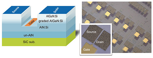
Staying at the forefront of materials research—Could you tell us about your achievement in 2022, which has been widely reported in the mass media? In 2022, to further reduce power losses of power devices, which are an essential component for using clean energy, we demonstrated—the world’s first—operation of a transistor using AlN (Fig. 1). Silicon (Si) is the main material used in semiconductor power devices, which are widely used in home electronics, personal computers, smartphones, server equipment, and electric vehicles. Using a wide-bandgap semiconductor with a high breakdown voltage*2 makes it possible to reduce the loss and increase the breakdown voltage of power devices. Accordingly, power devices using wide-bandgap semiconductors, such as silicon carbide (SiC) and gallium nitride (GaN), are being developed.
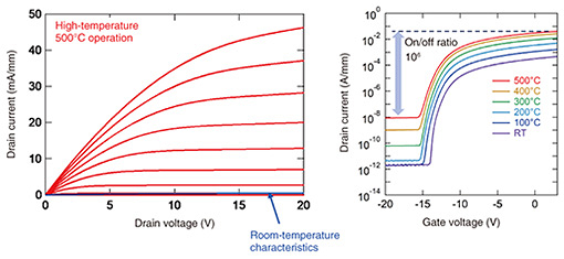
The use of ultrawide-bandgap semiconductors, which have higher breakdown voltages than wide-bandgap semiconductors, is expected to further improve the performance of power devices. Ultrawide-bandgap semiconductors include AlN, diamond, and gallium oxide (Ga2O3). If power devices using AlN, which has the highest breakdown voltage of any semiconductor, could be fabricated, it is theoretically expected that power loss could be reduced to less than 5% that of Si-based devices, 35% of SiC-based devices, and 50% of GaN-based devices. Among ultrawide-bandgap semiconductors, AlN is advantageous in that (i) devices can be fabricated on large wafers, which are necessary for industrial applications, and (ii) various device structures can be fabricated by forming a heterojunction between AlN and GaN. However, AlN power devices have rarely been reported, and the characteristics of the devices that have been developed have not been outstanding. By combining technologies that we have accumulated over the past 20 years, we developed a metal-organic chemical-vapor-deposition (MOCVD) system for fabricating high-quality AlN and succeeded for the first time in the operation of AlN transistors with good characteristics. The current-voltage characteristics of our AlN transistor showed a linear increase in current due to its good ohmic characteristics and an extremely small leakage current*3. Its breakdown voltage, which is an important factor in the performance of power devices, was as large as 1.7 kV. We also confirmed that our AlN transistor, unlike conventional semiconductor materials, can operate stably at high temperatures. Specifically, its performance improved at high temperature; namely, the drain current increased about 100 times at 500°C than at room temperature. Even at 500°C, the leakage current was kept extremely small at 10−8 A/mm. As a result, the on/off ratio of our AlN transistor was very high, over 106, even at 500°C (Fig. 2).
—You are highly regarded both in Japan and abroad for your advanced research and technological capabilities. Thankfully, our research results have been globally recognized. In 2011, at the age of 37, I received the Young Scientists’ Prize, the Commendation for Science and Technology by the Minister of Education, Culture, Sports, Science and Technology. The prize is awarded to young researchers under the age of 40 who have achieved outstanding results from their research—such as exploratory research and research from an original viewpoint—that demonstrates a high level of research and development capability. In the same year, I also received the Young Scientist Award at the International Symposium on Compound Semiconductors (ISCS), the top international conference on compound semiconductors, which is a gateway to success as a researcher in this field. It is an award for achievements in the field of compound semiconductors by scientists under the age of 40. In 2012, I received the Best Paper Award at the International Workshop on Nitride Semiconductors (IWN), an international conference with more than 1000 participants, and in 2019, I received the Japan Society for the Promotion of Science (JSPS) Prize for pioneering research on wide-bandgap semiconductor UV LEDs.
Quantity creates quality—Would you tell us what you value as a researcher? I try not to take for granted what is considered common sense or established theory or what is written in textbooks. I say that because things written in the textbooks are the solutions found by the means available at the time of writing. Therefore, I explore other possibilities while referring to textbooks and work with both my head and hands, that is, I think and experiment a lot. I ponder a problem over and over to find a solution. Sometimes I’m driven by my intuition in a way that I’m not even aware of, and say to myself, “This might work.” At such times, by intently conducting experiments with a “Let’s try it!” attitude, you can sometimes get good results. I respect the Nobel Prize laureate Dr. Hiroshi Amano, who invented the world’s first technology for creating high-quality GaN crystals necessary for blue LEDs. He overturned the established theory in the field that “blue LEDs cannot be made from GaN.” He believed in the potential of a material that no one else would pay attention to according to conventional theory and continued to conduct more than 1500 experiments with GaN. This perseverance led to great success. I think it must have been quite stressful for him until he got successful results. However, research activities are an act of attempting to solve problems that no one has yet answered, so it is not surprising that they often don’t succeed quickly. Nowadays, everyone talks about efficiency in regard to everything; however, materials research involves low-key efforts, and some things can only be revealed by doing a lot of work. Although it is said that “quality” is important in research, I believe that only when you pursue research through quantitatively large amount of effort, your sense is refined, and you can accumulate experience and knowledge, you will be able to understand what determines the quality of the research. In that sense, it is very important for researchers to work in an environment in which their long-term commitment is appreciated. NTT Basic Research Laboratories provides such an environment, for which I am grateful. —What are the responsibilities and joys of a researcher? It is a joy for a researcher to be able to stand at the forefront and take on the challenges that people say “cannot be done,” it is “just a dream,” “difficult,” “unintelligible” or “impossible.” It is the responsibility of researchers to propose and explore new possibilities through such challenges. Having curiosity and peers is crucial for conducting such research activities. When I was younger, I wanted to handle the entire research process by myself. However, I have learned through experience that by cooperating with many people, we can accomplish great things. In basic research, it is highly likely that new things will be created through multiple approaches of various experts using their techniques and ideas. The ideas of young people can be especially invigorating. I want to be an “eternally young researcher” who continues to take up challenges without fear of failure; at the same time, I want to be a “visible researcher.” That is, I want to be a researcher who learns from the achievements of my predecessors and, while passing those achievements on, builds up my own originality and strengths as a researcher so that people will recognize me as “Yoshitaka Taniyasu is the one for this research.” To all young researchers, let’s pursue our research activities with conviction and determination while keeping with interest and curiosity as our driving force. ■Interviewee profileYoshitaka Taniyasu received a B.E., M.S., and Dr. Eng. in electrical engineering from Chiba University in 1996, 1998, and 2001. He joined NTT Basic Research Laboratories in 2001, where he has been engaged in wide-bandgap semiconductor research. He received the Young Scientist Award at the 2007 Semiconducting and Insulating Materials Conference, the Young Scientist Award of the ISCS 2011, the Commendation for Science and Technology by the Minister of Education, Culture, Sports, Science and Technology of Japan (the Young Scientists’ Prize) in 2011, and the JSPS Prize in 2019. |
||||||||