|
|||||||||||
|
|
|||||||||||
       |
Feature Articles: Technology Development Trends of the IOWN 2.0 Era—From Communications to Computing Vol. 24, No. 4, pp. 30–37, Apr. 2026. https://doi.org/10.53829/ntr202604fa3 A High-capacity, Energy-efficient Photonics-electronics Converged Switch with PEC-2AbstractIn IOWN (Innovative Optical and Wireless Network) 2.0, the practical deployment of a photonics-electronics convergence (PEC) device is being pursued as a key PEC technology capable of dramatically reducing power consumption of the computing interconnect. This article first reviews the evolution of PEC technologies to date then explains the technical details of PEC-2, which is under development for application in the computing domain. This article also introduces a PEC switch equipped with PEC-2, which is being developed for use as a computing interconnect, along with its application at Expo 2025 Osaka, Kansai, Japan. Finally, future prospects toward commercialization are discussed. Keywords: IOWN, photonics-electronics convergence, disaggregated computing
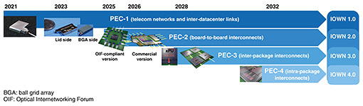
1. Optical communications and photonics-electronics convergence technologyNTT has been promoting optical transmission for several decades with the objective of advancing communication infrastructure. Compared with electrical signals, optical signals exhibit extremely low loss during transmission, offering the major advantage of stable, long-distance delivery with minimal attenuation. To fully leverage this characteristic, devices known as optical transceivers play a critical role in optical communication systems. Optical transceivers function as interfaces that convert electrical signals into optical signals and vice versa, serving as key components that connect information processing equipment to optical networks. Optical transmission using optical transceivers had been applied primarily to long-haul communications. However, its application has expanded to short-reach communications within datacenters. In modern datacenters, where massive volumes of data are exchanged between servers, transmission based solely on electrical signals is beginning to face limitations in terms of power consumption. Thus, the advantages of optical transmission are gaining increasing attention even in short-distance domains. Applying optical technologies to even shorter-reach data transmission is expected to enable further performance improvements. Against this background, NTT is focusing on photonics-electronics convergence (PEC) technology, which integrates electrical information processing with optical transmission. PEC contributes to reducing the overall power consumption of optical communication systems and positioned as a core technology for the actualization of the Innovative Optical and Wireless Network (IOWN), the next-generation network concept proposed by NTT. 2. NTT’s PEC technologyPEC technology integrates electronic circuits and optical circuits into a single platform, enabling the compact and highly efficient integration of optical transceiver functions. NTT collectively refers to the devices developed using this technology as PEC devices and has been advancing their practical deployment in stages in alignment with the IOWN vision. Figure 1 shows the roadmap of NTT’s PEC devices. In IOWN 1.0, digital coherent optical transceivers incorporating PEC-1 were introduced in All-Photonics Network (APN) services, which began commercial operation in 2023. Compared with conventional optical networks, these transceivers enable highly efficient and stable long-distance transmission, contributing to improvements in communication quality that form the foundation of IOWN.
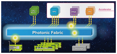
For IOWN 2.0, research and development (R&D) has progressed to extend PEC technology beyond the network domain into the computing domain, where large-scale data processing is executed. In datacenters, data traffic has been increasing rapidly, making power consumption a critical issue. To address this challenge, low-power, short-reach PEC-2 devices are being developed to construct high-capacity, energy-efficient interconnects, and efforts are underway to commercialize technologies that support the computing infrastructure of IOWN 2.0. Looking ahead to IOWN 3.0 and beyond, even more compact and lower-power devices—PEC-3 and PEC-4—are being developed to extend optical connectivity further into the interior of computers, including interconnections between semiconductor packages and within packages. Through this expansion of optical interconnects, NTT seeks to fundamentally transform computer architecture. 3. Computing applications of PEC technologyThe rapid advancements in artificial intelligence (AI) have driven unprecedented growth in data generation and computational demand, causing the volume of information handled by datacenters worldwide to increase exponentially. Achieving high computational performance requires enormous amounts of power; thus, datacenter energy consumption has become a serious global challenge. A particularly critical issue is that, alongside the increase in data volume, continued improvements in semiconductor performance have led to a sharp increase in the power required for data transmission. In conventional computing systems, data have primarily been transmitted as electrical signals between servers and between racks. However, with the development of AI and the spread of large-scale distributed processing, communication distances have become longer, and the volume of transmitted data has increased, pushing electrical transmission close to its physical limits. In electrical data transmission, power consumption increases rapidly as signal frequency increases and as transmission distance becomes longer. This behavior is an unavoidable consequence of the fundamental physical constraints of electrical interconnects. Looking ahead to a future with even higher signal frequencies and larger data volumes, the resulting growth in power consumption is emerging as an unavoidable problem. Against this background, PEC technology, which replaces electrical transmission with optical transmission, has attracted significant attention. Optical transmission enables high-frequency signals to be carried over long distances with low loss, making it possible to suppress the steep increase in power consumption that becomes problematic in electrical transmission. By leveraging optical interconnects, it becomes possible to sustain high-performance computing environments while dramatically reducing power consumption, an approach that is drawing strong global interest [1]. PEC is not only a means of reducing power consumption; it also fundamentally enhances communication performance, thus serves as a key technology for elevating the overall capabilities of computing systems. 4. Computer architectures leveraging PEC technologyIn current computing systems, the performance demands of applications are increasing faster than the performance improvements of computing semiconductors. Therefore, the traditional design approach of densely integrating high-performance resources such as graphics processing units (GPUs) within a single server chassis is becoming insufficient to meet emerging requirements. In AI training and large-scale data processing, massive volumes of data must be exchanged across multiple servers, and the disparity in communication characteristics between intra-server and inter-server connections has emerged as a new bottleneck. Inter-server networks exhibit higher latency and lower power efficiency than internal buses, making it difficult to handle resources in the same way as those within a server. Conventional architectures have thus been compelled to incorporate a wide variety of computational resources within each server to achieve higher performance. However, this approach is inefficient in terms of cost, power consumption, and redundancy. To address these challenges, we proposed an optical disaggregated computer architecture, as illustrated in Fig. 2. This architecture leverages PEC technology to connect computational resources across server boundaries with high bandwidth and low latency, enabling them to be operated as if they were part of a single large-scale computer system [2].
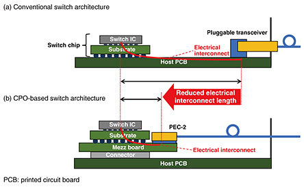
In this architecture, resources are managed on a pool basis rather than on a per-server basis, enabling flexible composition of optimal accelerators and memory according to the requirements of each workload. Furthermore, accelerators need not be general-purpose devices; instead, application-specific integrated circuits (ICs) can be deployed and used intensively, enabling both high performance and high efficiency in computation. Because this approach requires the exchange of massive amounts of data among distributed resources, optical interconnects that simultaneously deliver high bandwidth, low latency, and low power consumption are essential. It is in this context that the value of PEC technology is most fully demonstrated. 5. PEC-2 technologyOne implementation approach attracting significant attention for PEC is co-packaged optics (CPO), the standardization of which has been discussed within the Optical Internetworking Forum (OIF). By placing optical transceivers in close proximity to semiconductor ICs, CPO dramatically reduces the length of high-speed electrical interconnects that were essential in conventional pluggable transceiver architectures, thus fundamentally addressing issues of signal loss and power consumption. The PEC-2 technology under development by NTT also adopts this CPO approach. In the 3.2-Tbit/s CPO Implementation Agreement published by OIF, application to 51.2-Tbit/s-class Ethernet switches is envisioned [3]. This concept is based on arranging multiple CPO modules around the switch chip, minimizing electrical interconnect length to the greatest extent possible and enabling high-density, large-capacity switches with low power consumption. Figure 3 compares a conventional switch architecture with a CPO-based switch architecture. In conventional architectures, pluggable transceivers are typically installed on the front panel, and the long electrical interconnects between the switch chip and transceivers consume significant power, becoming a major obstacle to higher data rates.
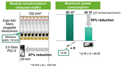
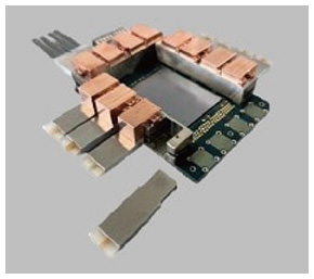
In CPO-based architectures, however, electrical-to-optical signal conversion is executed in close proximity to the switch chip, enabling optical interconnects to be deployed extensively within the chassis. Even when handling the same aggregate bandwidth, power consumption can thus be significantly reduced. Ethernet switches using CPO based on OIF specifications are under active development by multiple vendors, and their adoption as a standard architecture for next-generation network equipment is rapidly accelerating. 6. Development of a PEC-2-based PEC switch prototype and its deployment at Expo 2025NTT has advanced device technologies on the basis of a 3.2-Tbit/s CPO configuration compliant with OIF specifications. For PEC-2 module, silicon photonics technology is used to densely integrate optical modulators and receivers, while advanced signal processing implemented with a digital signal processor enables efficient conversion between electrical and optical signals. Each PEC-2 module supports 32 channels, achieving an aggregate bandwidth of 3.2 Tbit/s and supporting 100-Gbit/s PAM4 (four-level pulse amplitude modulation) signals. For the optical interface, OIF-compliant fiber pigtails are used, enabling a single module to provide eight channels equivalent to 400GBASE-DR4 output. Figure 4 compares PEC-2 modules with conventional pluggable transceivers required to achieve the same bandwidth. Because a single PEC-2 module provides 3.2 Tbit/s, it is equivalent to eight 400-Gbit/s pluggable transceivers. In terms of module size, PEC-2 enables an 87% reduction. Because PEC-2 satisfies the maximum power consumption specified by the OIF standard, it can deliver this bandwidth at 48 W, representing a 50% reduction compared with eight conventional pluggable transceivers consuming 12 W each.
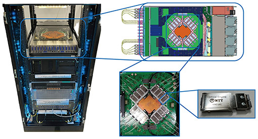
Using these PEC-2 modules, NTT fabricated a prototype PEC switch. By integrating PEC-2 modules in close proximity to a switch chip with a throughput of 51.2 Tbit/s, a switch system capable of forwarding Ethernet frames has been developed. As shown in Fig. 5, this switch was prototyped in a form factor suitable for a 19-inch rack, and stable operation of the high-heat-generating switch chip and PEC-2 modules was achieved through an efficient cooling design combining air cooling and liquid cooling.
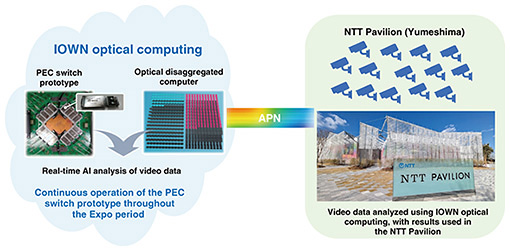
The front panel adopts 16-fiber multiple-fiber push-on (MPO) connectors, each accommodating two channels of 400GBASE-DR4. A total of 64 connectors enables an aggregate throughput of 51.2 Tbit/s, achieving a compact and high-density implementation. In addition to 400GBASE-DR4, the system also supports breakout to 100GBASE-DR. Through the use of an efficient cooling mechanism and a high-density front-panel optical interface based on MPO connectors, this PEC switch prototype achieves an extremely compact form factor of 2 rack units despite its very large switching capacity. This prototype was integrated and used as a computing interconnect within an actual optically disaggregated computer system. From April 13 to October 13, 2025, NTT exhibited a pavilion at Expo 2025 Osaka, Kansai, Japan where services based on IOWN optical computing were provided using an optically disaggregated computer architecture (Fig. 6). In this deployment, video streams from a large number of cameras installed across the venue were analyzed in real time using AI, and the results were incorporated into pavilion exhibits. Details of the Expo deployment are described in the feature article “Initiatives toward Social Implementation in the IOWN 2.0 Era” [4] in this issue.
Within this system, the PEC switch prototype played a critical role in efficiently distributing massive volumes of video data to multiple GPU accelerators. Stable operation throughout the six-month duration of the Expo demonstrated that PEC technologies, including PEC-2, possess the robustness and practicality required for real-world service environments. 7. Toward commercialization of PEC-2-based PEC switchesThe PEC switch prototype deployed at Expo 2025 used a CPO architecture compliant with OIF specifications; however, to move toward commercialization, further R&D is underway to achieve higher performance. Conventional Ethernet switches use pluggable optical transceivers that are inserted and removed from the front panel of the chassis. Because these transceivers are user-replaceable, faulty units can be easily swapped out, simplifying maintenance and repair. In a CPO configuration, however, the PEC-2 modules, which are functionally equivalent to conventional optical transceivers, are solder-mounted inside the chassis, in close proximity to the switch chip. They thus cannot be easily replaced. Maintenance requires stopping operation, disassembling the switch, and replacing the module, which increases both repair and operational costs. To address this issue, NTT Innovative Devices is pursuing practical deployment of a socket-type mounting structure that allows for attachable and detachable installation similar to pluggable transceivers while maintaining a CPO configuration in which the module is mounted directly adjacent to the switch chip (Fig. 7). In parallel, efforts are also focused on expanding the fundamental performance characteristics, including increased transmission capacity and significant reductions in power consumption. Development is underway to create a 6.4-Tbit/s PEC-2 module and integrate it with a 102.4-Tbit/s-class switch chip. This configuration aims to achieve a 50% reduction in power consumption compared with conventional switches that use pluggable transceivers. Regarding the commercial version of the PEC-2 module incorporating these performance enhancements, preparations are currently underway to enable the provision of samples in 2026.
8. Future outlookThis article presented PEC technologies under study for application to computing systems. Leveraging its strengths in optical communications, NTT is advancing R&D on devices based on PEC technology that integrates electrical processing with optical transmission. These technologies have been systematized as PEC devices. In IOWN 1.0, PEC-1 was introduced into the APN. Beginning with IOWN 2.0, the scope of PEC is being expanded into the computing domain. As an initial step, R&D is focused on PEC-2 to achieve low-power, high-capacity interconnects. Looking further ahead, PEC-3 and PEC-4 aim to extend optical connectivity into semiconductor packages and eventually within packages, with the goal of fundamentally transforming computer architectures. Toward the commercialization of PEC-2, a prototype PEC switch equipped with a 3.2-Tbit/s PEC-2 compliant with OIF specifications was developed, and its effectiveness was verified through practical operation at Expo 2025. NTT will continue R&D to further enhance the performance of PEC-2 and accelerate its commercialization. References
|
||||||||||