|
|||||||||||||||||||||
|
|
|||||||||||||||||||||
       |
Feature Articles: Forefront Research on Ultrawide-bandgap Semiconductors Vol. 24, No. 6, pp. 48–53, June 2026. https://doi.org/10.53829/ntr202606fa6 Engineering of Novel Ultrawide-bandgap Nitride SemiconductorsAbstractWe describe the world’s first epitaxial growth of cubic boron scandium nitride (c-BScN) layers by magnetron sputtering. The Sc composition can be controlled by changing the growth temperature. From X-ray absorption fine structure measurements using synchrotron radiation and first-principles calculations, we found that Sc atoms substitute for B atoms. These results open the way for the development and application of c-BN-based heterostructures in power devices. Keywords: cubic boron scandium nitride (c-BScN), power devices, next-generation wide-bandgap semiconductors
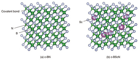
1. Novel nitride semiconductor materials for next-generation power device applicationsBoron (B) and nitrogen (N) are adjacent to carbon (C) in the periodic table. Carbon atoms form strong covalent bonds with one another, resulting in diamond, an extremely hard crystal. Boron and N atoms also form covalent bonds. They crystallize in the same cubic crystal structure*1 as diamond (Fig. 1(a)). This crystal is known as cubic boron nitride (c-BN), which has the widest bandgap energy (6.25 eV), therefore classified as an ultrawide-bandgap semiconductor*2. A wider bandgap generally leads to a higher breakdown electric field, which represents the maximum voltage a semiconductor can withstand. The breakdown electric field of c-BN is expected to be about 17.5 MV/cm, much higher than those of other materials. These characteristics make c-BN a promising material for power devices requiring high-voltage operation [1]. Power devices are electronic devices that convert electrical power between direct current (DC) and alternating current (AC) and control DC voltage levels. They are widely used in applications ranging from household appliances to inverters that drive the motors in trains and electric vehicles. Accordingly, reducing power loss in power devices is essential for global energy conservation and contributes significantly to a sustainable society. Silicon (Si) has long been the dominant semiconductor material for power devices. However, power devices based on wide-bandgap semiconductors*2, such as silicon carbide (SiC) and gallium nitride (GaN), are increasingly being researched and developed. Due to these materials having higher breakdown electric fields than Si, they can operate at higher voltages and more efficiently convert power with lower power loss. They are thus already being used in a broad range of applications, including electric trains and electric vehicles. Because the breakdown electric fields of c-BN is predicted to be more than five times higher than those of SiC and GaN, it is expected to exhibit even lower power loss and enable more efficient power devices. In addition, c-BN is chemically stable and highly resistant to high temperatures and radiation. These characteristics suggest it has the potential to be applied to not only conventional operating environments but also harsh environments such as space and nuclear power plants. NTT Basic Research Laboratories has long been studying the crystal growth of c-BN; c-BN has excellent semiconductor properties while its crystal growth is difficult. We have succeeded in epitaxially growing*3 c-BN layers and controlling their electrical conductivity by developing a unique growth method [2]. Cubic-boron-nitride-based ternary alloy materials also need to be grown for electronic device applications. These materials are formed by replacing some of the B atoms with other elements while maintaining the cubic structure of c-BN. One major advantage of such alloy materials is that their physical properties can be continuously tuned by changing the atomic composition. For this reason, semiconductor heterostructures*4 containing ternary alloy materials are widely used in various devices, including electronic devices, light-emitting devices, and sensors. We have thus been studying the crystal growth of cubic boron scandium nitride (c-BScN), a candidate ternary alloy material in the c-BN system (Fig. 1(b)). Scandium nitride (ScN) is a cubic crystal and has two polymorphs: the zinc-blende structure and rock-salt structure. These polymorphs differ markedly in their electrical properties, exhibiting bandgap energies of approximately 2.5 and 0.9 eV, respectively. In ternary c-BScN alloys, which are composed of c-BN and ScN, the bandgap energy can be continuously tuned over a wide range from 6.25 to 0.9 eV by adjusting the B and Sc composition. If electrons or holes can be confined near the interface of a heterostructure consisting of c-BScN and c-BN and used as a conduction channel, this material system is expected to enable low-loss power devices that can exploit the advantages of c-BN semiconductors.
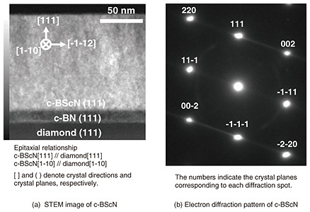
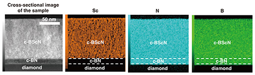
2. Epitaxial growth of c-BScNWe have recently epitaxially grown c-BScN layers for the first time on the basis of our c-BN crystal-growth technology and controlled the composition of these layers [3]. Diamond, which has the same crystal structure and a similar lattice constant, was used as the substrate for c-BScN growth. Magnetron sputtering*5, a technique widely used in industrial fabrication processes, was also used. For this study, a c-BN buffer layer was first grown on a diamond substrate, and a c-BScN layer was subsequently grown on the buffer layer. To investigate how c-BScN layers grow, we used scanning transmission electron microscopy (STEM), which enables crystal structures and stacked layers at the atomic scale to be directly observed by transmitting an electron beam through an ultrathin specimen. As shown in Fig. 2(a), c-BN and c-BScN layers were successfully formed on a diamond substrate. Figure 2(b) shows a selected-area electron diffraction*6 pattern obtained from the c-BScN layer. This result indicates that the c-BScN layer was epitaxially grown while inheriting the crystal structure of the diamond substrate. We also examined how Sc was distributed in the c-BScN layer by elemental mapping using STEM combined with energy-dispersive X-ray spectroscopy (EDS) (Fig. 3). By detecting element-specific X-rays emitted from a specimen under electron-beam irradiation, EDS can identify which elements are present. The analysis detected B and N in the c-BN buffer layer, and B, Sc, and N in the c-BScN layer. Scandium was uniformly distributed throughout the c-BScN layer, with no noticeable local segregation. These results show that a c-BScN layer with uniform Sc incorporation was epitaxially grown on the diamond substrate.
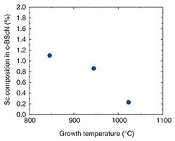
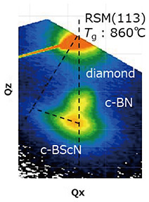
Figure 4 shows the dependence of Sc composition on growth temperature. The amount of Sc supplied during growth was kept constant at each temperature. The Sc composition was estimated by X-ray reciprocal space mapping (RSM), a crystal structure analysis technique, as shown in Fig. 5. The results revealed that lower growth temperatures led to more Sc being incorporated into the c-BScN layer. For example, the Sc composition in the sample grown at 860°C was about 1.1%. Such compositional control is important for intentionally designing the electrical and mechanical properties of materials and provides an important basis for future device applications. At growth temperatures above 1100°C, however, ScN with the rock-salt structure formed as separate phase instead of homogeneous c-BScN alloy. These results indicate that increasing the growth temperature enhances ScN formation via phase separation, thereby reducing the Sc composition in BScN.
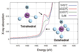
3. Characterization of bonding states in c-BScN using synchrotron radiationTo investigate in detail how Sc atoms are bonded in c-BScN layers, we carried out X-ray absorption fine structure (XAFS) measurements at NanoTerasu, a high-brightness synchrotron radiation facility. XAFS is a powerful technique that enables us to focus on a specific element and examine what types of atoms surround it, how they are arranged, and how they are bonded. X-ray absorption near-edge structure (XANES), the near-edge region of XAFS, is particularly sensitive to bonding and the coordination environment, making it useful for clarifying how Sc atoms are incorporated into the crystal structure of the novel material c-BScN. Such analysis requires synchrotron radiation with both high brightness and tunable X-ray energy. By taking advantage of the high-brightness synchrotron radiation available at NanoTerasu, we were able to conduct precise XANES measurements with a high signal-to-noise ratio even for elements in nanometer-scale ultrathin layers. As shown in Fig. 6, the Sc XANES spectrum of c-BScN exhibits a characteristic peak around 4490 eV, which is absent in ScN, indicating fourfold coordination of Sc atoms in c-BScN. To clarify in more detail where Sc atoms are incorporated in the c-BScN crystal, we also carried out first-principles calculations. First-principles calculations are theoretical methods that predict the behavior of atoms and electrons directly from the laws of physics on the basis of quantum mechanics, without relying on experimental parameters. Using this approach, we can determine which atomic configurations are energetically stable and what types of bonding states are likely to form. For this study, we simulated the XAFS spectra of c-BScN crystals for two cases: one in which Sc atoms replaced N atoms and another in which Sc atoms replaced B atoms. The results indicate that the simulated peak intensity and energy position for Sc substitution at the N site differed significantly from the experimental spectra. In contrast, the simulated peak shape for Sc substitution at the B site agreed well with the experimental results. Taken together, these experimental and theoretical results suggest that Sc atoms in c-BScN layers are incorporated by replacing B atoms in the zinc-blende crystal lattice. The knowledge obtained in this study will be useful for not only applying c-BScN but also exploring other c-BN-based ternary alloy materials. More broadly, designing conditions that enable different elements to be stably incorporated into the crystal lattice of metastable-phase materials provides important pathway for discovering new materials.
4. Summary and prospectsWe epitaxially grew c-BScN layers for the first time on diamond substrates by magnetron sputtering. We also found that the Sc composition can be controlled by adjusting the growth temperature. By combining XANES measurements using synchrotron radiation and first-principles calculations, we clarified that Sc atoms are incorporated at B sites in the c-BN lattice. We will further improve the properties of c-BScN by increasing its Sc composition and explore power device applications using c-BN-based heterostructures. References
|
||||||||||||||||||||