|
|||||
|
|
|||||
        |
Rising Researchers Vol. 24, No. 7, pp. 8–14, July 2026. https://doi.org/10.53829/ntr202607ri1  A Leap Forward in Ultra-high-speed Optical Modulation and Demodulation Technology for Achieving High-capacity, Long-distance TransmissionAbstractAs Internet data traffic continues to increase, technological advancements are continuously driving the development of communication technologies that are faster and offer higher capacity. However, handling the exponential increase in data traffic—for reasons such as the digitalization of business, growth of cloud services, popularization of remote work, and advancement in artificial intelligence—cannot be achieved overnight, even through continual technological innovation. For this article, we spoke with Distinguished Researcher Masanori Nakamura, a leading figure in ultra-high-speed optical modulation and demodulation technology, which is being researched and developed for handling the current increase in Internet traffic. Keywords: digital coherent technology, DSP-LSI, electrical-band multiplexing and demultiplexing
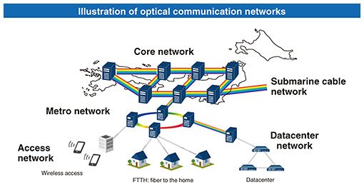
To deliver more information faster, further, and more accurately—What research are you currently conducting? Today, businesses rely on a wide range of hardware—from personal computers, smartphones, and tablets to Internet-of-Things devices—and the volume of data they handle, including high-resolution photos and videos, sales data, and customer-purchase data, keeps growing, so Internet traffic is surging. As artificial intelligence (AI) is being developed by various companies and its performance improves, and as it becomes commonplace, it is expected that communication volume will increase even more. In response to this increase in communication volume, it has become essential for us, as providers of infrastructure to meet this demand, to deliver more information faster and over longer distances. Let me first explain optical communication networks. Current optical communication networks have a hierarchical structure (Fig. 1). Data transmitted from homes and offices are aggregated in the access network then progressively bundled and transmitted to the metro network (metropolitan network) and core network (intercity network). This approach reduces the overall cost of the network and improves efficiency by transmitting data from many users together on high-capacity lines. Consequently, the transmission capacity required inevitably increases with each higher-level network. These higher-level networks use wavelength-division multiplexing (WDM), which bundles multiple wavelengths into a single optical fiber and transmits them simultaneously. By increasing the amount of information that can be carried via each wavelength, it is possible to increase overall network capacity, and the technology currently used to increase transmission capacity per wavelength is called digital coherent technology.
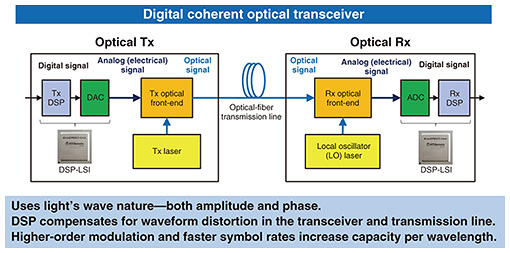
One of my research areas is the study of signal-processing algorithms used by digital signal processing large-scale integrated circuits (DSP-LSIs), which are central elements of digital coherent technology, and I’m also involved in developing and improving these devices. —Would you tell us about digital coherent technology, which is the core of your research? As an optical transmission technology, digital coherent technology combines DSP technology with coherent communication, which uses the phase and polarization of light. Under ongoing research and development, it is a key technology for increasing the speed, capacity, and distance of optical transmission. As shown in Fig. 2, on the data-transmission side, the data to be sent are converted into a signal suitable for modulation by a transmitter (Tx) DSP unit. That signal is then converted into an analog (electrical) signal with a digital-to-analog converter (DAC). Finally, the signal is transmitted as an optical signal with a Tx optical front-end, which modulates the information via laser light. The optical signal that arrives via an optical-fiber transmission line is demodulated into an analog electrical signal with the receiver (Rx) optical front-end, converted into a digital signal with an analog-to-digital converter (ADC), and the original data are then restored by correcting distortion with an Rx DSP unit.
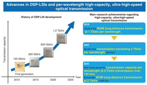
The key feature of digital coherent technology is the use of a local-oscillator laser light source on the receiving side that allows for both the amplitude and phase of the light to be accurately sensed (read). This feature enables higher-order modulation, which allows for more bits of information to be transmitted with a single signal change. Transmission capacity per wavelength is determined by the product of the amount of information transmitted by this higher-order modulation and the number of times the signal is changed per second (the symbol rate), so it is important to increase both the former and latter values. In fact, the functions of the Tx DSP, DAC, ADC, and Rx DSP are all integrated in a single semiconductor chip, DSP-LSI, which is the core device for digital coherent optical transmission. —What is a DSP-LSI? A DSP-LSI is an LSI specialized for DSP. DSP technology is widely used in communication fields, including wireless communications, and in optical communications, DSP-LSIs compatible with digital coherent technology have been in practical use since 2010. When I joined NTT in 2013, the first-generation DSP-LSIs had just been put into practical use, and development of the second generation was underway. The first-generation DSP-LSIs had a transmission capacity of 100 Gbit/s per wavelength, but their capacity has increased with each subsequent generation to 200 Gbit/s then 600 Gbit/s (see Fig. 3, left). With each generation, the technology to correct waveform distortion occurring in optical fibers by using DSP has matured, and the next challenge was to further improve transmission capacity and transmission distance.
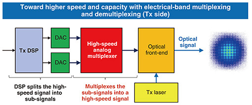
At that time, my initial approach was applying information theory. The application of information theory to optical communications was still in its early stages. My research focused on improving the arrangement of signal points when transmitting information via optical signals in a manner that enabled the transmission of more data over longer distances under the same conditions. Transmission performance depends on how the signal points, represented by a combination of light amplitude and phase, are arranged and how frequently each signal point is used. Today, such methods based on information theory are widely used for optical communications. I then expanded my research to include not only distortion in optical fibers but also technology using DSP for accurately estimating and compensating for deviations from the ideal state of electronic and optical devices used in optical transceivers. Each block shown in Fig. 2 (DAC, optical front-end, ADC, etc.) has its own unique characteristics, and as the modulation order and symbol rate increase, their effect on the signal becomes greater, thus high-precision correction by DSP becomes increasingly important. In addition to my research on significantly increasing transmission capacity per wavelength (by increasing the symbol rate), I’m currently working on improving performance and reducing power consumption by optimizing signal-processing algorithms. Achieving even greater capacity through a virtuous cycle of research and development—Would you tell us about any difficulties you encountered in your research and any challenges you anticipate facing in the future? I work in two areas: research to push the transmission capacity per wavelength ever higher, and development to bring DSP-LSIs into practical use. Pursuing the two together is a real strength: insights from research are fed directly into development, while the problems we encounter in development raise the questions that drive our next research—a virtuous cycle. However, advancing research and development in parallel is demanding, in different ways on each side. On the research side, the pressure comes from the intensity of global competition. Even after setting a world record in optical transmission, we can never ease up because a rival group may surpass it at the very next international conference. On the development side, the strain comes from having to do more in less time. The cycle for bringing DSP-LSIs to practical use keeps shrinking, and we have recently been developing two types of DSP-LSIs almost simultaneously—DSP-LSIs for long-distance, high-capacity systems and low-power DSP-LSIs for datacenters. Because research and development must advance at the same time, the time we can spend on experiments often gets squeezed into the period just before academic-conference submission deadlines, so managing our time is a constant balancing act—but one we take on gladly, because the payoff is real. The results obtained from both research and development are significant. Regarding research, we achieved the world’s first WDM long-distance transmission at 1 Tbit/s per wavelength in 2019; the world’s first transmission exceeding 2 Tbit/s in 2022; and set a new world record for transmission capacity (2.5 Tbit/s per wavelength) in 2025. We also demonstrated WDM long-distance transmission at 2 Tbit/s in 2025 (Fig. 3, right). The insights gained from this research have directly translated into development; specifically, we developed a DSP-LSI that achieves transmission at 1.2 Tbit/s per wavelength (Fig. 3, left). It is because of this virtuous cycle that we value keeping both wheels—research and development—turning. As we push transmission capacity even higher, we run up against a fundamental bottleneck: the bandwidth of the DAC/ADC that converts between the DSP signals and analog signals. The operating speed of DACs and ADCs using the currently dominant complementary metal-oxide-semiconductor (CMOS) technology is approaching its limit, which is expected to become a bottleneck in terms of symbol rates. We are therefore developing a method called electrical-band multiplexing and demultiplexing that uses high-speed analog circuits that operate at speeds exceeding what CMOS can achieve, combines multiple DAC outputs on the transmitting side, and separates and captures the received signal on the receiving side by using multiple ADCs. The configuration of the Tx unit is shown in Fig. 4. This method achieves symbol rates that exceed the bandwidth of DACs and ADCs, so we can push the limits of transmission capacity per wavelength even further. These high-speed analog circuits are designed and fabricated by NTT Device Technology Laboratories, and we incorporate them into optical transceivers. Drawing on the results of our transmission experiments, we feed requirements and points for improvement back to NTT Device Technology Laboratories. Our approach involves optimizing the entire optical transmission and reception system by using the above-mentioned device-compensation technology using DSP to estimate and compensate for deviations from the ideal state of the analog circuit. My research on electrical-band multiplexing was recognized with the 2025 Optica Tingye Li Innovation Prize, an international award given to young researchers in the field of optical communications.
—Would you tell us about your research prospects? Ultra-high-speed optical modulation and demodulation technology, which enables high-capacity, long-distance transmission, is directly linked to the core networks and inter-datacenter communication infrastructure that underpin the Internet. Due to the spread of high-definition video streaming and remote work as well as the rapid expansion of generative AI, communication traffic has continued to increase. Regarding generative AI, massive amounts of data are constantly moving between datacenters for training of large language models and the subsequent inference, and the bandwidth demand for datacenter interconnect is expanding at an unprecedented pace. To meet this demand, it is necessary to increase the transmission capacity per optical fiber significantly, and our efforts to maximize transmission capacity per wavelength are central to that. NTT’s Innovative Optical and Wireless Network (IOWN) aims to provide a low-latency, high-capacity network based on photonics-electronics convergence technology. In other words, ultra-high-speed optical modulation and demodulation technology directly underpins the high-capacity optical transmission that IOWN aims to deliver. In that sense, I believe it will be a key pillar in building the next-generation networks envisioned with IOWN. Going forward, we will further advance optical transceiver systems by integrating ultra-high-speed analog-circuit technology and DSP technology. As transmission capacity increases, two things are becoming increasingly important: technologies that use DSP to compensate for deviations from the ideal state of analog circuits, and new system architectures for efficiently handling ultra-wideband signals. My goal is to increase transmission capacity per wavelength and more efficiently achieve the high-capacity transmission required by next-generation backbone networks. I also envision the practical application of electrical-band multiplexing and demultiplexing through collaboration with multiple research laboratories and aim to accelerate the aforementioned virtuous cycle of research and development while contributing to the implementation of next-generation optical communication infrastructure that supports the growing demand for communications. —What are your impressions of NTT Network Innovation Laboratories, where you work? NTT Network Innovation Laboratories is unique in that, although it belongs to NTT Science and Core Technology Laboratory Group—which is devoted primarily to fundamental research—we also pursue development aimed at practical application. My impression is that we are striving to be at the forefront worldwide in terms of both research and practical application within an atmosphere where people can freely discuss issues across specialized fields. Following my personal motto, “enjoy trial and error,” I find it interesting to test my own predictions then think about what to do next according to the results. The unique cycle at NTT Network Innovation Laboratories, where research findings are applied to development and development challenges become new research themes, is what drives us to continue our efforts in research and development. Another characteristic of the Laboratories is the flexibility it offers in choosing between remote work and working at the office in accordance with the research and development phase and one’s lifestyle. Personally speaking, I prefer to think with my hands on experimental apparatus and value ideas that emerge from face-to-face discussions in front of a whiteboard, so I basically come to the office every day to work on research and development. Across the entire NTT Network Innovation Laboratories, numerous researchers are conducting a wide range of research related to the core of future networks, including high-capacity, ultra-high-speed optical transmission technology, photonic networks, and next-generation wireless systems. In parallel, development is underway to connect the results obtained from this research to actual communication systems. My research group includes researchers specializing in optical modulation and demodulation technology and DSP technology as well as experts in optical fiber transmission. We also work closely with analog circuit specialists at NTT Device Technology Laboratories, the optical device development team at NTT Device Innovation Center, and DSP-LSI development team at NTT Innovative Devices Corporation. The performance of an optical transmission system is not determined with individual technologies alone; rather, the design of the entire system, which consists of DSP units, analog circuits, and optical devices, is crucial for maximizing system performance. It is therefore common practice to bring together expertise from multiple specialized fields in research and development. NTT’s research on optical transmission has a major strength in its ability to combine expertise in each field with a comprehensive view of the entire system, and I believe that NTT Network Innovation Laboratories plays a hub role in facilitating such combinations.
—Finally, what is your message to our readers and students? Research in the field of optical communications has both theoretical and engineering aspects. Sometimes, predictions are based on theory then verified experimentally, and sometimes new hypotheses are born from measurement data. The fact that there isn’t simply one way to approach this field makes it so interesting. I majored in astrophysics at university, and I started working in optical communications after joining NTT. It’s a field where people from different backgrounds can thrive, and I feel that having a different perspective is often an advantage. Optical communication systems involve a wide range of technologies such as signal processing, information theory, semiconductor devices, and optics. At first, I struggled with the sheer number of things to learn, but that situation also means that the joy of learning new things never ends. NTT’s research on optical communications has been at the forefront worldwide since its early days. Within this environment, I experience the thrill of competing for world records, and I find great satisfaction in the speed at which the technologies that I’ve worked on are put to practical use. Of course, I can’t do everything alone; our results come from collaboration with many people including researchers within NTT as well as partners and collaborating companies. I also gain valuable inspiration from interacting with overseas rivals at international conferences. Optical communications are the foundation of the social infrastructure that supports the Internet, and in the era of rapidly advancing AI, expectations for even greater capacity are rising in this field. I want to continue working in collaboration with many people, so if you are interested, I’d be happy to work with you. This invitation isn’t only for those already drawn to this field; even if you feel it isn’t relevant to you because your expertise lies elsewhere, I’d encourage you to first experience the research environment through an internship at one of NTT laboratories [1]. When you get your hands dirty, you will find that your knowledge and perspective can be useful in unexpected places. Reference
■Interviewee profileMasanori Nakamura graduated from the Department of Applied Physics, School of Advanced Science and Engineering, Waseda University in 2011. He completed a master’s degree in physics and applied physics at the Graduate School of Advanced Science and Engineering, Waseda University in 2013. He joined Nippon Telegraph and Telephone Corporation (NTT) the same year, where he has been engaged in research on high-capacity, long-distance optical transmission using ultra-high-speed digital coherent technology. He obtained a Ph.D. in engineering from the Graduate School of Engineering, Osaka University in 2021. He has received the 2016 IEICE Communications Society Optical Communication Systems Young Researchers Award, the 2022 IEICE Communications Society Optical Communication Systems Best Paper Award, the 2022 67th Maejima Hisoka Award, and the 2025 Optica Tingye Li Innovation Prize (OFC). |
||||