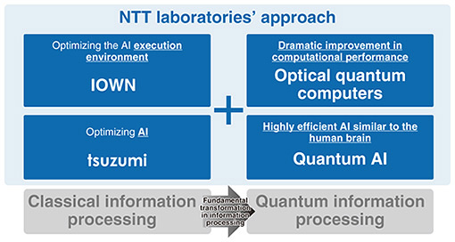
At NTT laboratories, we are currently pursuing three key strategic themes: the Innovative Optical and Wireless Network (IOWN), the generative artificial intelligence (AI) model “tsuzumi,” and optical quantum computers. This article reports the progress of each of these research themes.
I will first explore why NTT laboratories are researching these themes to give some background. AI is evolving tremendously, but let’s set that aside and look at this situation from the perspective of AI development. The current AI development can be viewed as creating an ultra-large capital-intensive industry. Thus, let’s consider this ultra-large scale in terms of numbers.
Enormous costs are required for AI development and training. According to the AI Index Report published by Stanford University, even GPT-4, a model 1.5 generations before the current GPT-5.5, has several trillion parameters and costs approximately 15 to 20 billion yen to develop. This amount is only for a single development run; if the model is rebuilt multiple times, for example, with each version update, the total development cost can be about 10 to 100 times higher.
From the perspective of power consumption, creating a large language model (LLM) of GPT-4 class requires about 40 GWh of electricity, an enormous amount of energy equivalent to the output of 40 nuclear power plants running for an hour. When ChatGPT’s LLM executes inference during actual use after training, it is said to consume 2.9 Wh, which is about 10 times higher than the amount consumed by conventional Google search, 0.3 Wh.
The amount of investment made to create LLMs and other AI models is also huge. For example, private company investment in the United States has reached 285 billion dollars, compared with 1.1 billion dollars in Japan, about 1/260th of the U.S. figure.
To meet increasing AI needs, demand for datacenters is surging. For example, datacenters consuming 123 GW are expected to be constructed in the United States by 2035. In Japan, power demand for datacenters is forecast to reach 6 GW by 2034.
Let’s take a look at the number of engineers and researchers. Specifically, let’s examine the number of co-authors of major papers on generative AI. While a typical academic paper requires about five to at most ten authors, about 1350 researchers were involved in writing papers on Google’s Gemini, according to data from 2023.
As we have seen, AI is taking on the characteristics of a capital-intensive, or even resource-intensive, industry. Looking toward its future evolution, however, we now have to reconsider what kind of research and development we should pursue. We need to ask ourselves, for example, whether we should continue to increase computing resources. We should also think from a national standpoint and ask whether Japan can increase such resources on its own and if increasing the resources truly benefits humanity and the Earth. Thus, our research and development strategies should be carefully planned.
If AI development accelerates further, classical information processing may no longer suffice to provide adequate solutions. To address this, NTT is expanding the scope of research and development to quantum information processing by adding two other approaches: optical quantum computers and quantum AI. The former is to aim for dramatic and overwhelming improvements in computational performance, while the latter is for designing AI that emulates the efficiency of the human brain. Thus, our strategic approach consists of these four major pillars for research and development to address the evolution of AI that will require vast resources.
2.1 IOWN
To understand IOWN, we first have to learn about the difference between electric and optical transmission properties. In electrical wiring, power consumption increases rapidly when the transmission distance exceeds approximately 15 cm. Increasing the operating frequency from 10 to 20 GHz results in further large power consumption. Optical wiring, however, has excellent characteristics in that power consumption remains almost unchanged over longer distances and stays relatively low even at high operating frequencies. Thus, IOWN has been developed by leveraging the characteristics of optical wiring and can be briefly described as overcoming the limitations of information and communication processing through conversion into optical wiring from electrical wiring. It is considered to provide a means of balancing the two conflicting requirements, transmission performance and power consumption.
The key point of IOWN is where optical conversion takes place. IOWN is divided into four phases according to the domain where photonics is incorporated (Fig. 2). IOWN 1.0 means the utilization of photonics within networks. It makes communications between datacenters fully photonic. In IOWN 2.0 and later, photonics is brought into computers. More specifically, in 2.0, communications will be made fully photonic in servers, that is, between the boards of servers inside datacenters. Then in 3.0, communications will be fully photonic between chips on a board. Finally in 4.0, communications will be fully photonic between dies in chips, the smallest units of a chip. By introducing photonics into very local domains in this manner, we pursue achieving both high transmission performance and low power consumption.
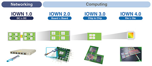
Fig. 2. IOWN roadmap.
IOWN 1.0 has been available as a commercial service since its launch in 2023 by NTT EAST, NTT WEST, and NTT DOCOMO BUSINESS. As a use case of the All-Photonics Network (APN) based on IOWN 1.0, enterprise services, particularly those leveraging ultra-low latency, have been deployed in a variety of situations.
We believe that the APN is significantly effective not only for end-to-end enterprise services but also for datacenter businesses. The current most challenging problem with datacenters is the shortage of available land. It is said that 88% of existing datacenters in Japan are concentrated in the Tokyo metropolitan and Osaka regions. Given this, securing land for building new datacenters is a major issue.
A potential solution to this challenge that is attracting attention is watt-bit collaboration (Fig. 3). Datacenters tend to be located in urban areas because users strongly demand it for accessibility. Power lines indicated with the red line in the figure, the so-called watt section, thus need to be extended over considerable distances, increasing their costs. To counter this, the APN can be installed to minimize latency, enabling datacenters to be located in suburban areas. This means they are brought closer to power plants. By shortening the distance of the red power line, the costs for total cable installation can be reduced. One calculation estimates that the costs could be reduced to about one hundredth, so there are high expectations for watt-bit collaboration and installation of datacenters in suburban areas.
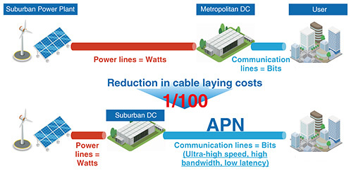
Fig. 3. Watt-bit collaboration.
An advanced version of this can also hold promise. While the above-described watt-bit collaboration is static, dynamic watt-bit collaboration may also be possible. For example, if there are datacenters in Kyushu, Hokkaido, and the Kanto region (the region including the Tokyo metropolitan region), and power generation in Kyushu is low, processing can be transferred to Hokkaido from Kyushu to ensure continuous operation. Therefore, the overall utilization rate of renewable energy can be dramatically increased, which produces another benefit of the large-capacity, low-latency APN. We are currently conducting various demonstration tests to verify the effectiveness of dynamic watt-bit collaboration.
Next, I explain IOWN 2.0, a phase where photonics is making inroads into computing. There are high expectations for applying IOWN 2.0 inside AI datacenters. Systems for developing large-scale AI models require configurations that can collectively switch a very large number of graphics processing units (GPUs). If there are 1000 GPUs, and each one of the 1000 GPUs communicates with the other 999, the amount of communication reaches approximately one thousand squared. Switching GPUs at extremely high speed is a challenge for overall system performance. InfiniBand (NVIDIA) and Ultra Ethernet are currently used for ultra-high-speed switches for AI datacenters. To replace them, we are aiming to develop a photonics-electronics convergence (PEC) switch using an IOWN 2.0-based PEC device that can achieve overwhelmingly low power consumption and fast processing.
The reason our PEC-2 switch can achieve low power consumption is illustrated in Fig. 4. The figure on the left shows a side view of a conventional optical switch. A transceiver is inserted into the front of the switch, and the pink part is an application-specific integrated circuit (ASIC) for the switch. The wire up to the transceiver is optical, but an electrical wire is still used for the 300-mm section from the transceiver to the ASIC. In this 300-mm section, power consumption surges when the data rate exceeds 10 Tbit/s, as described earlier. NTT’s PEC-2 switch on the right can reduce the electrical wire to only 30 mm, reducing power consumption. The commercial version of the switch is scheduled to be released at the end of fiscal 2026. We are working toward commercialization in partnership with Broadcom, which is in charge of designing the ASIC chip, NTT Innovative Devices manufacturing the optical engine and switch modules, and Accton Technology assembling the switch box.
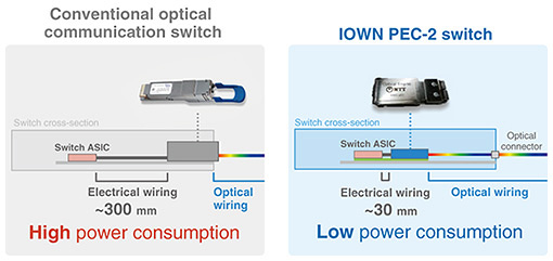
Fig. 4. Reduced power consumption of IOWN PEC-2 switch.
2.2 tsuzumi
Next, I will introduce tsuzumi as an example of improving the efficiency of AI. In 2023, NTT developed its own LLM, tsuzumi . At that time, the model had 7 billion (B) parameters, but to further improve its performance, we developed a 30B-parameter model called “tsuzumi 2”. The reason we focused on 30B is that a model of this size can run on a single current-generation GPU. Using just one GPU means that the model can be easily run on premises, that is, on a company’s own server. This reduces costs and power consumption, and because no information needs to be sent outside the company, it also enables a highly secure AI environment.
Some may argue that a smaller model cannot achieve high performance, but by specializing in Japanese language, we have achieved world-class performance in Japanese-language processing despite the model’s smaller size. Benchmarking Japanese-language knowledge, analytical ability, instruction-following capability, and safety has shown that tsuzumi 2 outperforms globally renowned LLMs of a similar size and achieves performance comparable to GPT-5, which is several times larger than tsuzumi 2.
tsuzumi 2 is also designed as a specialized model to perform well in fields such as finance, local government, and healthcare. For example, we evaluated how much additional training would be required for the model to pass the 2nd-grade Certified Skilled Professional of Financial Planning exam in the financial sector. Google’s Gemma required training on about 1900 questions to achieve a passing score, whereas tsuzumi 2 achieved a passing score after training on only about 200 questions, which we believe represents an approximately tenfold improvement in learning efficiency.
On May 19, 2026, we announced an update to tsuzumi 2 that added a visual-reading-comprehension feature (Fig. 5). As shown in the text below the graphs, visual reading comprehension refers to the ability of an LLM to analyze documents and slides containing figures and tables, as well as graphs and charts. As shown in the same figure, benchmarking across a range of tasks has demonstrated that tsuzumi 2 delivers the best performance among models in its class and achieves performance comparable even to larger models.
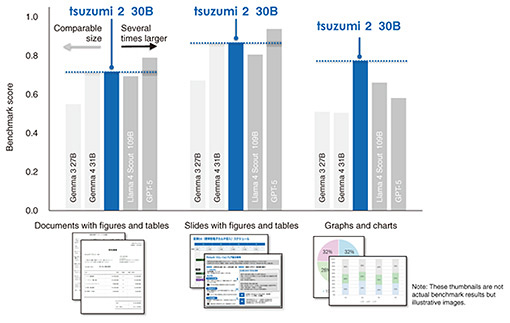
Fig. 5. World-class visual reading comprehension performance.
The final feature is that tsuzumi 2 is a Japanese AI (Fig. 6). The term sovereignty has been used frequently in recent years, and this is also an area of focus for tsuzumi . Anthropic recently released a highly capable AI called Mythos, which is said to have made it easier to discover vulnerabilities in various types of software. Due to security considerations, Mythos is currently being offered and disclosed only to a limited number of companies. In Japan, for example, you may have heard reports that the three megabanks are in negotiations, including with the government, to gain access to Mythos. Given this, we need to seriously consider these issues from the perspective of economic security. What if access to AI from other countries were unilaterally restricted? What if Japanese culture and language were manipulated or interfered with by AI from other countries? And what if the number of companies or engineers capable of developing AI in Japan were to decline or even disappear altogether? We place great importance on Japanese AI and AI sovereignty. Sovereignty means safeguarding our own language and culture. Sovereignty means selecting our own training data and using them to train AI models. Sovereignty means determining the development process, including the order and timing of development. We also want to protect licensing sovereignty. AI has become a strategic resource, and access to it could be restricted at any time or subject to extremely high licensing fees. Sovereignty also means preserving and passing on technological expertise. With these considerations in mind, NTT has developed tsuzumi independently from scratch, with the aim of safeguarding Japan’s economic security.
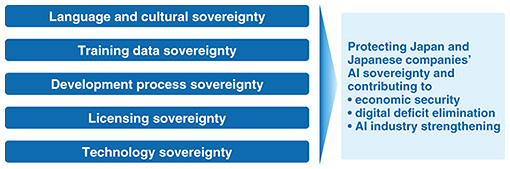
Fig. 6. Japanese AI.
2.3 Optical quantum computers
I will now explain the optical quantum computers we are developing. There are various types of quantum computers, and we are researching an approach known as optical quantum computing. I would like to explain how it basically works. Quantum light is first generated. This requires a device called a quantum light source. This quantum light takes the form of optical pulses. We then create quantum entanglement and form clusters of entangled quantum states, much like weaving threads together to make fabric. Roughly speaking, the process involves programming the quantum states with values such as 0 and 1 then measuring them to execute the computation all at once.
To improve the performance of an optical quantum computer, the quantum light source needs to be extremely high quality and high speed. Larger entanglement clusters also increase the amount of computation that can be executed at once, enabling large-scale computation. The faster the measuring instruments become, the faster the computation becomes. These three factors represent major challenges in optical quantum computers.
Figure 7 shows the hardware and software configurations used to build an optical quantum computer. On the left is the quantum light source, and the red line to its right represents the optical system, which consists of components such as optical fibers and mirrors. The system also includes an observation/control device, quantum-specific computation functions, and software.
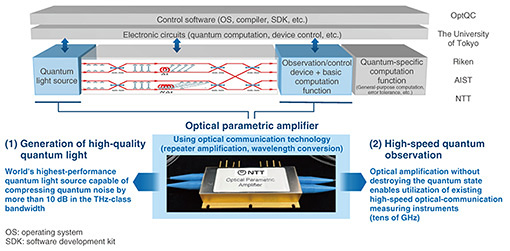
Fig. 7. NTT’s technology: optical parametric amplifier.
The blue sections are key. NTT’s strengths in this area lie in its quantum light source and observation device technologies. The device used for this is an optical parametric amplifier, which was originally used for repeater amplification and wavelength conversion in optical communications. We found that this device was extremely well suited to quantum computing. After making modifications for use in quantum computers, we achieved outstanding performance and, in collaboration with Professor Furusawa of the University of Tokyo, are now achieving world-leading results.
There are various approaches to quantum computing (Fig. 8). For example, there are superconducting, neutral-atom, ion-trap, and optical approaches, the last of which is the approach we are pursuing. When comparing these approaches, the overwhelming advantage of the optical approach lies in its operating environment. The superconducting approach requires cryogenic temperatures and a vacuum. You may have seen quantum computers that look like chandeliers and are extremely large. Most of what you see is actually the cooling system, with a small quantum chip inside. With the superconducting approach, increasing the number of qubits requires scaling up the entire apparatus. For example, a 1000-qubit system could require an area equivalent to several tennis courts, which is why scalability is considered a major challenge. In contrast, the optical approach operates at room temperature and atmospheric pressure, giving it a significant advantage in terms of scalability.
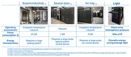
Fig. 8. Only the optical method operates at room temperature and atmospheric pressure.
Another major advantage is its high compatibility with optical communication technologies. Such technologies—including light source technology, wavelength conversion technology, low-loss optical fibers, multicore fibers, and wavelength-division multiplexing—can also be used in optical quantum computers. The high-speed optical detection technology used in optical communication receivers can also be applied to quantum measurements. A major advantage, therefore, is that technologies originally developed through investment in optical communications can be applied to optical quantum computers with only minor modifications.
Toward the practical application of optical quantum computers, NTT has formed a business partnership with OptQC, a startup founded by Professor Furusawa of the University of Tokyo, a leading expert in optical quantum computing. Together, NTT and OptQC aim to bring optical quantum computers into practical use, with milestones set for 2027, 2030, and 2040 (Fig. 9). By 2027, a 10,000-qubit system will be able to solve large-scale optimization problems in areas such as communications and transportation. By 2030, a 1-million-qubit system will make it possible to reduce the environmental impact of fertilizer production. With a 100-million-qubit system, it will be possible to customize new drugs for each of the world’s 8 billion people. These advances are expected to help address such societal challenges.
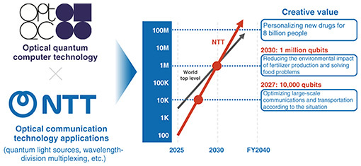
Fig. 9. Toward practical applications of optical quantum computers.
2.4 Relationship between IOWN and quantum
Finally, I will summarize the relationship between IOWN and quantum (Fig. 10). IOWN 1.0 through 4.0, which I introduced earlier, are in the optical transmission domain. The scale becomes progressively smaller, from between datacenters to within chips, but the focus remains on the transmission of light. The next step is expected to be the evolution toward computation using light. NTT has also begun research on optical transistors, optical logic gates, and neural networks. Although this involves computation using light, it is still primarily classical computing. To achieve even greater performance, quantum properties are essential. Optical quantum computing brings us to the optical quantum computers I introduced earlier. We envision evolving beyond IOWN 4.0 in these directions and expanding the use of light into the computing domain.
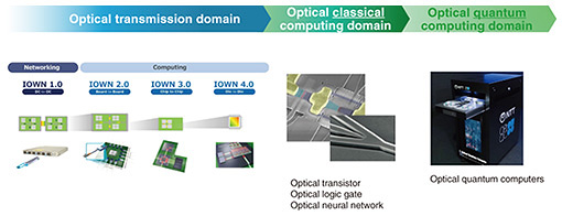
Fig. 10. Relationship between IOWN and quantum.
Given the current situation where extremely large resources are needed for the future evolution of AI, NTT’s research and development efforts focus on IOWN to improve the efficiency of the AI execution environment; tsuzumi, aimed at improving the efficiency of AI; optical quantum computers, which dramatically improve computational performance in the quantum domain; and quantum AI, which I wasn’t able to explain much today. Through these broad themes spanning both classical information processing and quantum information processing, we hope to contribute to a future AI-driven society.