|
|||||||||||||||||||||||||||||||||||
|
|
|||||||||||||||||||||||||||||||||||
       |
Selected Papers: Wide Area Ubiquitous Network Vol. 6, No. 3, pp. 40–46, Mar. 2008. https://doi.org/10.53829/ntr200803sp5 Low-power Circuit Techniques for Wireless Terminals in Wide Area Ubiquitous NetworkAbstractThis paper describes methods for reducing power consumption in terminals for the wide area ubiquitous network (WAUN). The importance of low-power operation and the impact of intermittent operation on terminal power consumption are discussed. A multithreshold CMOS (complementary metal oxide semiconductor) circuit scheme and a fast-locking phase-locked loop circuit scheme that greatly reduce the power consumption are presented. These techniques can extend battery life significantly. 
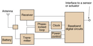
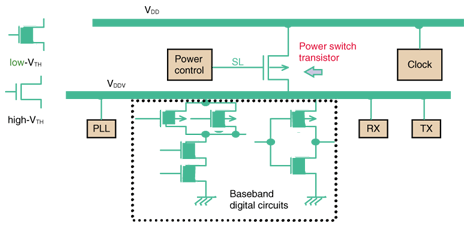
1. IntroductionA simplified block diagram of a terminal for the wide area ubiquitous network (WAUN) [1] is shown in Fig. 1. The terminal consists of radio frequency (transmitter (Tx) and receiver (Rx)) circuits, a phase-locked loop (PLL), a clock, baseband digital circuits, a battery, an interface for a sensor or actuator, and an antenna. To make a low-cost terminal, we must integrate almost all of the active circuits into a single-chip LSI (large-scale integrated circuit). Integrated wireless transceiver LSI technology makes it possible to eliminate many external components, so it is promising for making small, low-cost terminals. Components that cannot be integrated are the battery, sensor or actuator, and antenna. The antenna can be built on a board together with the LSI because the designed antenna gain is –15 dBi, which can be attained by using a printed pattern on the board. The interface to the sensor or actuator is typically a serial one having a low bit rate such as 9600 bit/s. Provided that it is small, a sensor or an actuator (for example, a single-chip temperature sensor) can be built on the terminal's board through customization of the interface. Thanks to its small size, a WAUN terminal containing a sensor or actuator could be installed in various places. On the other hand, if the sensor or actuator has complex functions and is not small, the WAUN terminal should be built into the sensor or actuator and could be connected using an adapter that converts the protocols used by the sensor/actuator and WAUN terminal. In this case, the WAUN terminal itself must be small enough to build into another device. Minimizing WAUN terminal size is therefore very important regardless of whether the sensor or actuator is simple or large and complex. Our target size for WAUN terminals is 10 cm3 or less. The main obstacle to such miniaturization is the size of the battery. In WAUN, an extremely large number of terminals will be widely distributed in various environments, including outdoors. Thus, the terminals must have small power supplies, such as coin batteries or thin-film batteries with a life of several years because the batteries cannot be recharged or replaced. Thus, lowering power consumption (and hence decreasing battery size) is a crucial issue in WAUN terminal development.
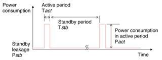
2. Intermittent operationClearly, extremely low-power operation of WAUN terminals cannot be attained with continuous operation. Therefore, we must consider intermittent operation at the cost of response time. Fortunately, WAUN services do not always need the quick response that mobile phone services do. This points to the possibility that the averaged power consumption could be reduced by decreasing the activity ratio, which, owing to the intermittent operation, could be set several orders of magnitude lower than that in cellular phone systems. Typical intermittent operation is shown in Fig. 2, where Pact and Pstb represent the power consumption in the active and standby periods and Tact and Tstb are the lengths of the active and standby periods. Average power consumption Pav is calculated as
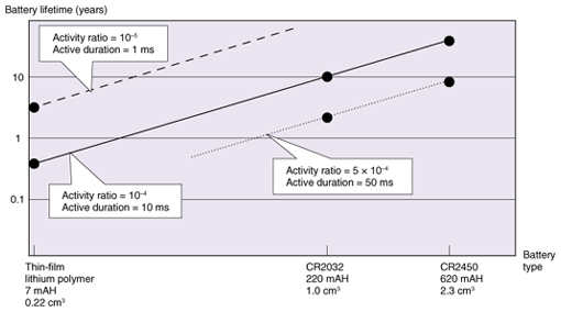
The above scenario, in which Pstb is negligible and Tact can be shortened to 1 ms, is rather an ideal one and actually beyond the capability of conventional technology. Considering these points, the next two sections describe two key techniques—a multithreshold complementary metal oxide semiconductor (MTCMOS) [2] circuit scheme for reducing Pstb and a fast-locking PLL circuit scheme for reducing Tact.
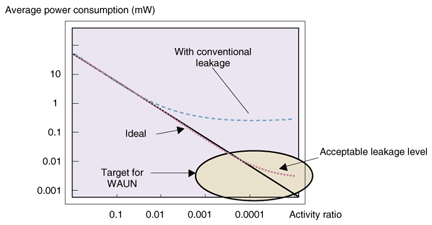
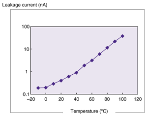
3. MTCMOSPower consumption is generally expected to be proportional to the activity ratio Ract. However, we cannot rely on this expectation for our target Ract because static leakage current could become the dominant component of the power consumption. It will be very difficult to achieve the target Ract by using conventional CMOS circuit technologies. The target Ract and the target leakage level are shown in Fig. 4, where we again assume that power consumption during the active period is 50 mW. In some cases, a terminal should have a kind of slow clock that continues to operate during standby, which could affect the standby power. However, slow-clock circuits usually consist of a small number of gates, which can have a fairly small current consumption of 0.1 µA [4]. On the other hand, the main circuits in wireless terminals have a large number of gates because they must provide complicated functions. Consequently, their leakage power is large. In addition, the static leakage always increases by one or two orders of magnitude when the ambient temperature rises from room temperature to about 85°C [5]. Since outdoor terminals may be set at various points, robustness against environmental temperature is a major issue. This means that we must keep the leakage low with a margin of at least two orders of magnitude. One of the most promising solutions is MTCMOS on silicon-on-insulator (SOI) technology [2], [3]. In this technology, low- and high-threshold-voltage MOSFETs (metal oxide semiconductor field effect transistors) are integrated in a single LSI. The low-threshold-voltage ones enhance speed performance, especially in RF circuits, while the high-threshold-voltage ones suppress standby leakage current during the sleep period. A power-switch transistor supplies the operating current to circuits in the active mode and cuts the leakage current in the sleep mode. The basic MTCMOS circuit scheme for wireless terminals is shown in Fig. 5. The main circuits are composed of MOSFETs with a low threshold voltage. The power terminals of the transistors are not connected directly to the power supply lines (VDD), but rather to virtual power supply lines (VDDV). The real and virtual power lines are linked by a power-switch MOSFET, whose threshold voltage is high enough to make the standby leakage current extremely low when the switch is off. We experimentally examined the leak-cut performance using a power switch fabricated in a CMOS/SOI LSI, which exhibited leakage of less than 1 nA at room temperature with sufficiently high current drivability of more than 30 mA. Its measured leakage current is shown in Fig. 6 as a function of temperature. These results indicate that this switch has a sufficiently large margin to achieve the target maximum leakage current of 1 µA.
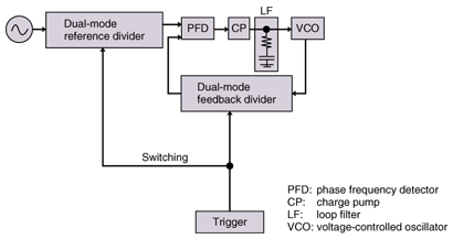
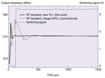
4. Fast-locking PLL circuitIn WAUN terminals, the active duration must be as short as possible to further lower the power, as explained in section 2. We can arrange protocols so that both the receiving (Rx) and transmitting (Tx) periods are decreased to slightly less than 1 ms, which seems to be the lower limit because it corresponds to a few symbols in the WAUN radio signal. Intermittent operation for carrier sensing is an example of such a short period. If the startup time of circuits becomes comparable to the Rx and Tx periods, power consumption in the startup period cannot be neglected. It is clear that the startup time must be much shorter than the active period. The most critical circuit is the PLL circuit, which generally has the longest acquisition time among RF circuits. Thus, we must develop a fast-locking PLL frequency synthesizer. For a PLL, when the damping factor ζ is constant, the acquisition time Tacq is inversely proportional to the natural angular frequency ωn [6]. Although increasing ωn is effective for obtaining a short acquisition time, a large ωn causes a large phase noise. An effective way to release the PLL from this restriction is to control ωn according to the operating state (acquisition or tracking). This is because a large phase noise is acceptable in the acquisition state when no data signal is being transferred. Methods for controlling ωn by switching loop circuits with analog blocks such as a loop filter have been introduced [7]–[9]. However, when the transmission gate transistor is switched, electrons that have accumulated in the transmission gate capacitor during the acquisition state are discharged, which leads to a fluctuation in the voltage of the loop filter. For this reason, PLLs inevitably suffer from the above switching noise. Generally, an elaborate structure is necessary to overcome this problem. Considering this background, our goal is to solve the trade-off between the acquisition time and phase noise with a simple structure. To overcome this trade-off and avoid the analog-switching noise, we devised a new PLL that uses a fully digital natural-frequency-switching technique. In this technique, ωn is controlled by switching only the division ratio of digital blocks, i.e., the reference divider and feedback divider. (Fig. 7) dynamically according to the relationship that ωn is inversely proportional to the square root of the division ratio. By switching only the digital blocks, we can avoid the noise caused by switching the loop filter to maintain ζ. The switching of the division ratio leads to a variation in ζ because ζ is inversely proportional to the square root of the division ratio, like ωn. Since the PLL characteristics (acquisition time and phase noise) strongly depend on ζ, our PLL should be switched within a limited value of ζ. We therefore determined ζ according to the following policy: In the acquisition state, from the viewpoint of fast locking, ζ=1 is generally valid [10]; in the tracking state, from the viewpoint of achieving low phase noise, 0.25 is valid. The ωn in the acquisition state can be five times as high as ωn in the tracking state. We chose a fractional ratio of 25, giving ωn priority over ζ in the acquisition state, and a phase frequency detector input frequency of 50 kHz in the tracking state. The voltage-controlled oscillator oscillates in the frequency range from 545 to 596 MHz, which corresponds to twice the carrier frequency of a WAUN terminal. Since the double-frequency signal is convenient for making quadrature signals for the demodulator in a receiver, we use a signal with this frequency range from the oscillator. The measured acquisition time in our fully digital switching mode is compared with that in the conventional integer-N mode in Fig. 8. The acquisition time for our PLL was 110 μs, which is about one-fifth that for the integer-N PLL. We verified that phase noise in the tracking state was not degraded. Moreover, because our PLL is digitally switched to avoid analog-switching noise, it stayed locked. The fast-locking PLL synthesizer using the fully digital natural-frequency-switching technique overcomes the trade-off between the acquisition time and phase noise and does not suffer from analog-switching noise. With this technique, we can achieve a startup time that is much shorter than the active period Tact, which corresponds to the ideal condition mentioned in section 2. This should enable us to use a thin-film battery as the power supply in a WAUN terminal.
5. ConclusionTwo key circuits techniques for WAUN terminals were presented. Because a WAUN terminal operates intermittently, the total power consumption of the terminal strongly depends on the standby leakage current and startup time of the circuits, so it is essential to minimize both. We showed that a multithreshold CMOS circuit scheme can attain sufficiently low standby leakage power of less than 1 µW, and a fast-locking PLL circuit scheme can attain a sufficiently short startup time of about 0.1 ms. These schemes are highly effective with intermittent operation and they can extend battery life to more than 10 years, even if a coin or thin-film battery is used. References
|
||||||||||||||||||||||||||||||||||