 |
|||||||||||||||||||||||||||||||
|
|
|||||||||||||||||||||||||||||||
       |
Selected Papers: Forefront of Basic Research at NTT Basic Research Laboratories Vol. 6, No. 8, pp. 13–20, Aug. 2008. https://doi.org/10.53829/ntr200808sp3 Nanoelectrode Lithography:
|
||||||||||||||||||||||||||||||

| † | NTT Basic Research Laboratories Atsugi-shi, 243-0198 Japan |
|---|
1. Introduction
Nanometer-scale patterning is needed to fabricate the nanometer-sized structures that are key structures in the fields of photonic crystals, quantum electronics, nanomechanical sensors, biochips, and information storage. Many kinds of patterning processes have been investigated for nanostructure fabrication, including electron beam (EB) lithography, X-ray lithography, and extreme ultraviolet lithography. However, the equipment required for flexible patterning with a reasonable throughput is currently very large. For the future development of nanotechnology, we need fabrication techniques that can be used easily and efficiently.
Considering the above background, nanoimprint technology [1]–[4] has recently been attracting a lot of attention in the fields of optical devices, mass storage media, electronic devices, and bio-applications. It uses a mold with a desired pattern. Since a pattern can be transferred by just pressing the mold against a target repeatedly, this technology provides an efficient and economical way to duplicate a pattern.
Nanoelectrode lithography also uses a mold with a desired pattern. However, it uses a conductive mold, and a voltage applied between the conductive mold and the target causes an electrochemical reaction on the surface of the target. This electrochemical reaction transfers the pattern to the target. For the electrochemical reaction, we can utilize an anodic oxidation of semiconductor or metal, which has been used in atomic force microscope (AFM) lithography [5]–[7]. We can categorize nanoelectrode lithography as chemical nanoimprint, while physical nanoimprint includes nanoimprint technology, which transfers the shape of the mold surface to the target.
In this paper, we discuss the features of nanoelectrode lithography.
2. Nanoelectrode lithography
The concepts of nanoelectrode lithography [8] and conventional nanoimprint are compared in Fig. 1. In conventional nanoimprint, the mold is pressed against the target, and the shape of the mold surface is physically transferred to the target surface to obtain a pattern with peaks and valleys. On the other hand, nanoelectrode lithography works by transferring a pattern on a conductive mold to a target via an electrochemical reaction. The conductive mold makes contact with the surface of a target, such as a semiconductor or metal layer. When a voltage is applied, current flows between the conductive mold and the target material. Then, an electrochemical reaction occurs on the target surface, for example, anodic oxidation of the semiconductor or metal. As a result of this electrochemical reaction, the pattern on the conductive mold is transferred to the target.
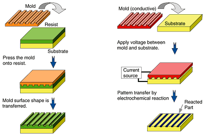
Fig. 1. Concepts of conventional nanoimprint (left) and nanoelectrode lithography (right).
Because nanoelectrode lithography involves an electrochemical reaction, it provides the following advantages. First, it can directly make an oxide pattern on the target, and the oxide pattern can be used directly as an etching mask for wet or dry etching of the substrate. This resist-less patterning should decrease the number of process steps. It could also improve the accuracy of pattern transfer and decrease the number of defects. In addition, the technique should eliminate the breakdown of the mold during the release procedure, which is a problem in conventional nanoimprint where the mold can break during the release procedure after adhering to the resist. Second, we can use a mold with a small etching depth and low aspect ratio, while conventional nanoimprint needs one with a large etching depth and high aspect ratio to obtain enough contrast in the depth of the transferred features on the resist. This characteristic lets us easily make a template with a small pattern size. Furthermore, it should be possible for the pattern on the mold used in the technique to be defined by the contrast in conductivity, and it can eliminate the etching process in the mold fabrication. Third, the technique does not deform the surface of a target. This characteristic should enable EB or AFM lithography to provide additional modification of the transferred pattern after nanoelectrode lithography. It should also be possible to repeat the nanoelectrode lithography. Such multiple patterning may enable us to fabricate a complex pattern by repeating the pattern transfer with a mold having a simple pattern.
3. Patterning of semiconductor by nanoelectrode lithography and fabrication of nanostructures
The feasibility of this concept has been confirmed by fabricating a silicon oxide pattern on a silicon substrate. Just as a conductive tip makes a pattern by anodic oxidation in AFM lithography [5], we can expect a conductive mold to make a pattern on a Si surface via anodic oxidation of Si. A conductive mold was obtained by EB lithography and etching on a conductive substrate. The etching process created a pattern consisting of projections and trenches on the surface of the conductive mold. When the conductive mold was brought into contact with the target, only the projections touched the surface of the Si target. Thus, the projections acted as conductive areas, and the trenches acted as insulating areas. The conductive regions of the conductive mold caused anodic oxidation on the Si surface, thus producing a SiO2 pattern.
In one of our experiments, we applied a voltage of 15 to 25 V between the conductive mold and Si substrate. Scanning electron microscope (SEM) images of the Si substrate after nanoelectrode lithography [8] are shown in Fig. 2. A line-and-space (L/S) and closely packed hexagonal pattern was successfully obtained and it matched the conductive mold pattern. This pattern is considered to originate from the SiO2. To confirm this, we etched a 500-nm-pitch L/S pattern with HF solution. This produced a topographical image of the L/S pattern with a pitch of 500 nm. The etching depth was 5 to 10 nm. The results show that a SiO2 pattern with a thickness of over 5 nm was successfully fabricated by nanoelectrode lithography.
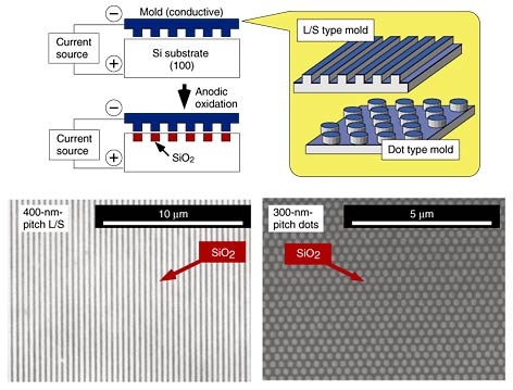
Fig. 2. SEM images of Si substrate after nanoelectrode lithography.
One possible application of a SiO2 pattern on a Si substrate is an etching mask. A thin SiO2 layer can act as an etching mask for the wet etching of Si with KOH [9]. We wet-etched a Si substrate in 0.8 N KOH aqueous solution for 45 s. An AFM image of the Si substrate after etching is shown in Fig. 3(a). A topographic image with a depth of 140 nm was obtained. This shows that the SiO2 pattern was deeply transferred to the Si substrate by KOH wet etching. The feasibility of using a SiO2 mask fabricated in this way as an etching mask for dry etching was also confirmed. An AFM image of a Si substrate after dry etching using fluorocarbon gas plasma is shown in Fig. 3(b). It shows that dry etching to a depth of 20 nm was accomplished with the etching conditions used here.
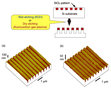
Fig. 3. AFM image of Si substrate after nanoelectrode lithography followed by (a) wet etching and
(b) dry etching.
4. Patterning of metal layer on substrate and fabrication of nanostructure
Patterning of a metal layer on a substrate may enable the fabrication of a metal oxide mask on a substrate. In addition, some metal oxides could show various types of functionality. Thus, metal layer patterning could broaden the applications of nanoelectrode lithography. This section describes an aluminum oxide mask fabricated on a Si substrate [10].
The experimental procedure and results are shown in Fig. 4. We deposited an Al layer with a thickness of 10 nm on a Si substrate. The conductive mold made contact with the surface of the Al layer. When a voltage was applied, current flowed between the conductive mold and the target. Then, the pattern on the conductive mold was transferred to the Al surface. Aluminum oxide was generated corresponding to the pattern on the conductive mold. To investigate the feasibility of using the fabricated metal oxide pattern as an etching mask for dry etching of the Si substrate, we removed the remaining metal part by wet etching.
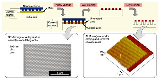
Fig. 4. Nanoelectrode lithography on metal layer.
We used a conductive mold with a closely packed hexagonal pattern. The fabricated pattern on the Al layer is also shown in Fig. 4. A 400-nm-pitch closely packed hexagonal pattern corresponding to the conductive mold pattern was fabricated. Then, wet etching with phosphoric acid removed the unreacted area. The reacted area remained after the wet etching, which shows that nanoelectrode lithography followed by wet etching can provide a metal oxide mask. Figure 4 also confirms that the oxide mask could be used as an etching mask for dry etching of the substrate.
5. Multiple patterning and fabrication of nanostructure
One possible advantage of nanoelectrode lithography is that it will enable us to overwrite a pattern because this technique does not deform the surface of the target during the patterning process. Multiple patterning was undertaken to confirm the feasibility of this [11]. The experimental procedure and results are shown in Fig. 5. First, nanoelectrode lithography was performed with an L/S-pattern conductive mold. Then, the process was repeated with the conductive mold rotated by 90°. Finally, a checkered pattern was fabricated. For the experiment, an L/S-pattern conductive mold with a pitch of 500 nm was used. SEM images taken after the first and second procedures are also shown in Fig. 5. A checkered pattern was successfully fabricated. The results show that nanoelectrode lithography allows multiple patterning. They also indicate that a pattern fabricated by nanoelectrode lithography can be modified by combining this approach with additional lithographic techniques.
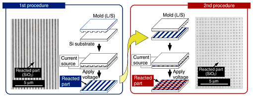
Fig. 5. Procedure of multiple patterning and results.
The fabricated checkered pattern can be used as a wet etching mask. A wet etching experiment was performed using a KOH aqueous solution. AFM 3D images of the Si surface after the etching process are shown in Fig. 6. As shown in Fig. 6(a), SiO2 layers generated in the first and second procedures additionally acted as an etching mask. This produced logical OR patterning. In Fig. 6(b), only the overlapping area of the SiO2 layers generated in the first and second procedures acted as an etching mask. Therefore, square projections remained on the surface. This shows that logical AND patterning can be achieved. The difference between the two results may be caused by the thickness of the SiO2 layer, so it may be possible to determine the final structure by choosing the process conditions.
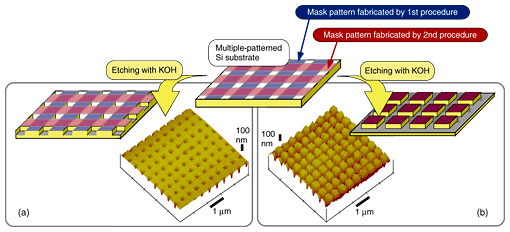
Fig. 6. AFM image of Si substrate after multiple patterning followed by wet etching: OR patterning (a) and AND patterning (b).
6. Development of mold with higher durability
In the experiment mentioned above, we used a conductive Si substrate with the desired pattern as the conductive mold. To obtain a conductive mold with higher durability, we investigated the mold material and fabrication process [12]. In addition to the requirements for a conventional nanoimprint mold, such as mechanical strength, ease of processing, and flatness, we need a material with good conductivity for this technique. Our choice for the mold material was sintered silicon carbide (SiC). It has high conductivity, and the mechanical strength of sintered SiC is higher than that of Si. A poly-SiC film was formed by low-pressure chemical vapor deposition (CVD) to obtain a flat surface on the sintered SiC. The voids existing in the surface of the sintered SiC could be covered with CVD poly-SiC films. After deposition, the surface of the poly-SiC film was polished. As a result, the flatness of the mold surface was better than 1 nm (Ra). The total resistivity of the mold was less than 0.01 ohm-cm. In addition to the advantages mentioned above, an evaluation of the contact angle suggested that a SiC mold should easily adsorb surface moisture, which plays an important role in the anodic oxidation of Si.
SEM images of the mold patterns after dry etching are shown in Fig. 7. Highly accurate dry etching enabled us to form a 60-nm-wide L/S pattern. In addition, patterns with a rectangular cross-section were obtained, as shown in Fig. 7. Thus, we successfully produced a mold with high conductivity and high mechanical strength.
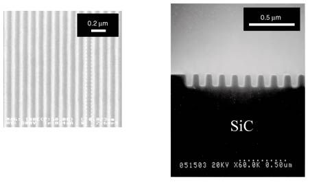
Fig. 7. SEM images of mold patterns: top (left) and cross-sectional (right) views. The top and cross-sectional views are 60- and 80-nm L/S patterns, respectively.
7. Development of nanoimprinter for device production
To apply nanoelectrode lithography to the production of actual devices, we constructed a nanoimprint tool called the Chemical Nanoimprinter [12]. Its construction is shown in Fig. 8. Uniform contact between a mold and a substrate was achieved by using a mold pressure adjustment system, which controls the pressure applied to each part of the mold. In addition to the contact control, we consider that moisture control for the mold surface is important. It may be possible to obtain a fine oxide pattern with good reproducibility if we can control the amount of moisture on the mold surface, which can be a medium in the anodic oxidation process. For this purpose, we managed the temperature and humidity in the chamber and the mold temperature. In this way, we were able to control the moisture adsorbed on the mold surface. Furthermore, this nanoimprinter has a step-and-repeat patterning system. The positioning stage has an accuracy of 10 nm or better using an ultrasonic motor. The accuracy of the stage lets us make a large-area pattern by repeating the pattern transfer with a small-area mold. This is one advantage of this patterning approach over the conventional physical nanoimprint.
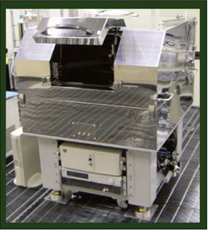
Fig. 8. Chemical nanoimprinter.
An SEM image of a Si surface patterned with the nanoimprinter and then wet etched in KOH aqueous solution is shown in Fig. 9. We confirmed that a 100-nm-wide line nanostructure and 100-nm-wide space nanostructure were successfully fabricated [12].
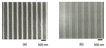
Fig. 9. SEM image of Si surface after patterning of 100-nm-wide lines (a) and 100-nm-wide spaces (b) followed by wet etching in KOH aqueous solution.
8. Conclusion
Nanoelectrode lithography enables us to make an oxide pattern directly on the surface of a semiconductor or metal layer. This resist-less patterning may provide a small feature size much more easily than the conventional nanoimprint technology. We also confirmed the feasibility of multiple patterning, which shows the possibility of post-nanoelectrode-lithography modification by other patterning methods. Furthermore, we can expect other features, such as pattern transfer from a mold without peaks and valleys.
We are currently conducting a detailed evaluation of the patterning process with the nanoimprinter, which is designed to control the contact and atmospheric conditions precisely. We hope that this patterning approach can contribute to device production and future progress of nanotechnology.
Acknowledgments
This work is partially supported by the New Energy and Industrial Technology Development Organization (NEDO).
References
| [1] | X.-M. Zhao, Y. Xia, and G. M. Whitesides, “Fabrication of three-dimensional micro-structures: Microtransfer molding,” Advanced Materials, Vol. 8, pp. 837–840, 1996. |
|---|---|
| [2] | A. Kumar and G. M. Whitesides, “Features of gold having micrometer to centimeter dimensions can be formed through a combination of stamping with an elastomeric stamp and an alkanethiol “ink” followed by chemical etching,” Appl. Phys. Lett., Vol. 63, No. 2002, 1993. |
| [3] | P. R. Krauss and S. Y. Chou, “Nano-compact disks with 400 Gbit/in2 storage density fabricated using nanoimprint lithography and read with proximal probe,” Appl. Phys. Lett., Vol. 71, No. 3174, 1997. |
| [4] | S. W. Pang, T. Tamamura, M. Nakao, A. Ozawa, and H. Masuda, “Direct Nano-Printing on Al Substrate using SiC Mold,” J. Vac. Sci. Technol. B, Vol. 16, pp. 1145–1149, 1998. |
| [5] | E. S. Snow, P. M. Campbell, and P. J. McMarr, “Fabrication of silicon nanostructures with a scanning tunneling microscope,” Appl. Phys. Lett., Vol. 63, No. 749, 1993. |
| [6] | A. Majumder, P. I. Oden, J. P. Carrejo, L. A. Nagahara, J. J. Graham, and J. Alexander, “Nanometer-scale lithography using the atomic force microscope,” Appl. Phys. Lett., Vol. 61, No. 2293, 1992. |
| [7] | Y. Matsuzaki, S. Hasui, S. Kamada, A. Yamada, and M. Konagai, “Improvement in Aspect Ratio of P-GaAs Oxide Fabricated by Atomic Force Microscope (AFM)-Based Nanolithography Using Pulsed Voltage,” Jpn. J. Appl. Phys., Vol. 40, pp. 4325–4327, 2001. |
| [8] | A. Yokoo, “Nanoelectrode Lithography,” Jpn. J. Appl. Phys., Vol. 42, L92–L94, 2003. |
| [9] | H. Sugimura, T. Yamamoto, N. Nakagiri, M. Miyashita, and T. Onuki, “Maskless patterning of silicon surface based on scanning tunneling microscope tip-induced anodization and chemical etching,” Appl. Phys. Lett., Vol. 65, No. 1569, 1994. |
| [10] | A. Yokoo, H. Namatsu, and M. Oda, “Nanostructured and Patterned Materials for Information Storage,” edited by Z. Z. Bandic, M. Rooks, R. Berger, and T. Ando (Mater. Res. Soc. Symp. Proc. 961E, Warrendale, PA, 2007), 0961–O10–01. |
| [11] | A. Yokoo, “Nanoelectrode lithography and multiple patterning,” J. Vac. Sci. Technol. B, Vol. 21, No. 6, pp. 2966–2969, 2003. |
| [12] | H. Namatsu, M. Oda, A. Yokoo, M. Fukuda, K. Irisa, S. Tsurumi, and K. Komatsu, “Chemical nanoimprint lithography for step-and-repeat Si patterning,” J. Vac. Sci. Technol. B, Vol. 25, No. 6, p. 2321, 2007. |
 |
|
|---|---|
 |
|