|
|||||||||||||||||||||||||||||||
|
|
|||||||||||||||||||||||||||||||
       |
Special Feature: Front-line Materials Research Vol. 8, No. 8, pp. 23–30, Aug. 2010. https://doi.org/10.53829/ntr201008sf5 Towards New Low-dimensional Semiconductor Nanostructures and New PossibilitiesAbstractThis article introduces our research on the bottom-up growth of semiconductor nanowires and an advanced investigation of their optical and electrical properties. We also describe the fabrication of various novel nanostructures that will help to promote nanowire applications and open up new opportunities. 
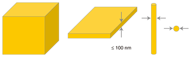
1. Nanoscience and nanotechnologyNanosystems, which are defined as having dimensions and/or characteristic lengths of between 1 and 100 nm, exhibit particularly distinctive and interesting physical properties, namely quantized energy levels, Coulomb blockades, and single-electron tunneling. These phenomena occur in structures small enough for quantum mechanical effects to play an important role. The fundamental study of the phenomena that occur in these 1–100-nm-scale structures has already evolved into a new research field known as nanoscience. New knowledge obtained at the nanoscale level has led to the creation of nanodevices based on new principles, including the single-photon emitter and the single-electron transistor. Research on nanostructures has contributed to the development of a number of current and emerging technologies in addition to assisting the progress of nanoscience. In microelectronics, smaller has always meant more components per chip, a faster response, lower cost, lower power consumption, and improved performance. In recent years, the miniaturization and production of microelectronic chips has been guided by a road map published by the Semiconductor Industry Association, which predicts that the metallic interconnect width of a dynamic random access memory (DRAM) device will reach 25 nm by 2015. The trend towards miniaturization will also apply to other technologies. The study of the control, formation, and fabrication techniques used for structures with dimensions in the 1–100 nm range is known as nanotechnology. Nanotechnology is related to a broad array of disciplines, including chemistry, biology, physics, computational science, and engineering. Like information technology, nanotechnology has the potential to affect virtually every industry, from aerospace and energy to healthcare and agriculture. 2. One-dimensional semiconductor nanostructures and their applicationsSemiconductors have provided extremely important research fields related to electronic and photonic device applications as well as to fundamental physics. Quantum mechanics is becoming very important as the semiconductor size approaches the nanoscale. One-dimensional (1D) semiconductor nanostructures such as nanotubes, nanorods, and nanowires have two dimensions smaller than 100 nm, as schematically shown in Fig. 1. Owing to their low dimensionality and quantum confinement phenomena, 1D nanowires are expected to exhibit certain distinctive and novel properties that differ from those of conventional bulk and thin-film materials. In addition to the well-known quantization of the energy level in nanostructures, these properties appear, for example, in relation to the melting point, thermal conductivity, quantized conductance, lasing threshold, and polarization of light emitted along the longitudinal axes in 1D nanostructures.
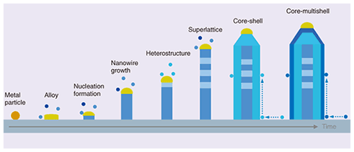
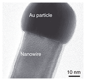
The potential uses of these nanostructures depend strongly on their quality and controllability; namely, the position, orientation, diameter, density, chemical composition, and crystal structure must be precisely controlled. Thus, it is essential to investigate the synthesis of semiconducting nanostructures for further fundamental studies and technological applications. 3. Synthesis approach for 1D semiconductor nanostructuresThe two principal ways of fabricating 1D semiconductor nanostructures are the top-down and bottom-up approaches. Top-down means that the nanostructures are fabricated from bulk crystals using, for example, lithographic techniques (electron beam lithography, nanoimprinting, etc.) and selective dry and wet etching. The crucial disadvantages of the top-down approach are its high cost and the damage induced. In contrast, the bottom-up approach constructs nanostructures by self-assembly. The vapor-liquid-solid (VLS) bottom-up approach has recently been widely used to synthesize 1D semiconductor nanostructures. A typical growth process is schematically shown in Fig. 2. It starts from the dissolution of gaseous reactants into metallic nanoparticles to form a metallic solution. Once the solution becomes supersaturated, a nucleus is produced; this nucleus then grows and nanowires subsequently form. A transmission electron microscopy (TEM) image of a nanowire tip is shown in Fig. 3, in which a gold (Au) particle and an underlying nanowire segment can be clearly seen. One can form a heterostructure by changing the source reactants. Superlattice nanowires can also be achieved by the periodic introduction of different source reactants. Moreover, by choosing appropriate growth conditions, we can grow epitaxial layers on the side walls of the nanowires by using conventional vapor phase epitaxy. As a result, one can achieve both axial and radial heterostructures, and this technique can grow various novel low-dimensional nanostructures.
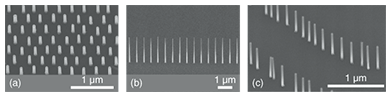
The nanowires grown by the VLS method are highly controllable because the nanowire size and site are directly controlled by using size-selective and site-defined metallic nanoparticles. By selecting an appropriate substrate orientation, one can grow nanowires vertically on the substrate to form a nanowire array. Scanning electron microscopy (SEM) images of a GaAs nanowire array and an InP nano-wire line grown from a Au-particle pattern defined by electron beam lithography are shown in Figs. 4(a) and (b), respectively. In contrast to Figs. 4(a) and (b), where we used fine lithographic patterns, we tried to form a self-assembled array of Au particles aligned on the atomic steps of a Si substrate surface [1], and the successful formation of GaP nanowire arrays by Au dot arrays self-assembled on the Si atomic steps is shown in Fig. 4(c) [2].
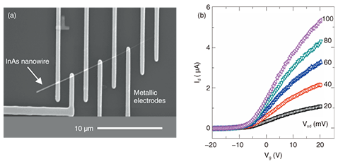
4. Electrical and optical properties of semiconductor nanowiresElectronic and optoelectronic devices have various applications ranging from household appliances to commercial systems for communications, computing, and medical services. Given the demand for ever more compact and powerful systems, there is growing interest in the development of nanoscale devices that provide new functions and/or greatly enhanced performance. Semiconductor nanowires are emerging as a powerful class of materials that, through their controlled growth and organization, are opening up substantial opportunities for the development of novel nanoscale photonic and electronic devices. In the following, we introduce their electrical and optical properties, which could lead to diverse and exciting future applications. InAs nanowires have become good candidates for high-speed nanoelectronics because of their high carrier mobility. We grew InAs nanowires with high crystalline quality by the Au-catalyzed VLS method, and then fabricated back-gated field-effect transistor (FET) devices. The InAs nanowires were mechanically removed from the as-grown samples and dispersed on a Si substrate covered with an insulating SiO2 layer. A number of metallic contacts were formed on a single nanowire by combining electron-beam lithography and metallic deposition techniques. The corresponding SEM image of the InAs nanowire-channel FET device is shown in Fig. 5(a). Typical drain current (Id)-gate voltage (Vg) characteristics of the device for various source-drain voltages at room temperature are shown in Fig. 5(b). We can see that the back gate voltage changed the carrier concentration in the InAs nanowire channel very effectively. This indicates that the InAs nanowires function as FETs. Using the transport characteristics, we can estimate the carrier concentration and mobility of the nanowire and then obtain feedback on the growth condition as regards doping to make nanowires with the desired electrical properties.
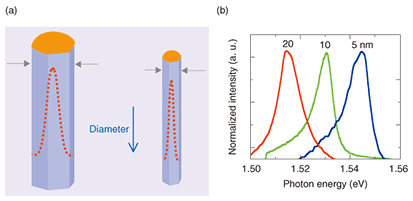
The optical properties of GaAs quantum nanowires embedded in AlGaAs barrier layers, which are usually formed on V-groove substrates, have been extensively studied for applications to optoelectronic devices such as quantum lasers and detectors [3]. By contrast, freestanding nanowires will provide novel and interesting physical properties because the surrounding medium (air or vacuum) has a considerably lower dielectric constant, so the electromagnetic fields are tightly confined within the nanowires. By using size-selective Au nanoparticles, we grew bare freestanding GaAs nanowires with controlled diameters. We observed that a single nanowire had a uniform diameter along its axis and included very few stacking faults. If the nanowire diameter is small enough, then, in principle, quantum mechanics becomes important and the quantum confinement effect causes the luminescence peak to shift to the high energy side, as shown schematically in Fig. 6(a). Indeed, photoluminescence measurements revealed a clear blue shift of the excitonic emission from single nanowires with decreasing diameter, as shown in Fig. 6(b) [4].
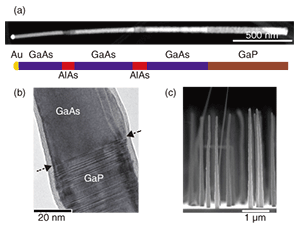
5. Heterostructure nanowiresSemiconductor heterostructures are extremely important in both fundamental physical research and device applications. Because they are 1D freestanding structures with nanoscale diameters, nanowires can endure significantly more strain both radially and axially than films. Heterostructures in semiconductor nanowires can therefore be formed without dislocations even in the case of materials that have a large lattice mismatch. This opens up substantial opportunities for various material combinations, including InAs/InP and GaAs/GaP. We have fabricated AlAs/GaAs/GaP heterostructure nanowires by the VLS method. A TEM image of a heterostructure nanowire and its compositional distribution are shown in Fig. 7(a). Despite there being a lattice mismatch between GaAs and GaP of as high as ∼4%, no dislocations were introduced into the GaAs segment, as can be seen from Fig. 7(b) [5]. We grew the nanowire heterostructures epitaxially on a Si(111) substrate because the contact between the nanowires and the Si substrate occurs in the nanoscale region, so it can endure a high strain [6], [7]. This makes it possible to integrate III-V compound semiconductor devices into Si-based technology, leading to Si-based optoelectronic integrated circuits.
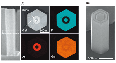
Radial composition modulation in nanowire structures provides another approach to enhanced performance and/or new functions. We have fabricated GaP/GaAs/GaP core-multishell nanowires by combining the VLS and subsequent vapor phase epitaxy growth techniques. Removal of the Au catalyst particle before shell layer growth makes it possible to form a flat top surface. A cross-sectional SEM image of the nanowire is shown on the left in Fig. 8(a). We characterized the internal core-shell structure by TEM observation using a thin slice of the single nanowire shown schematically by a dashed rectangle. The figures on the right in Fig. 8(a) show the corresponding TEM image and three elemental mappings, from which we can clearly see the compositional distribution [8]. Moreover, by combining the radial composition modulation and selective etching techniques, we formed a 3D nanostructure with a radial air-semiconductor periodic structure. A tilt-view SEM image of nanotubes with air gaps is shown in Fig. 8(b). A preliminary simulation indicates that the core-multishell nanowire structure with air gaps has a relatively strong photon confinement effect and can function as a photonic cavity [9].
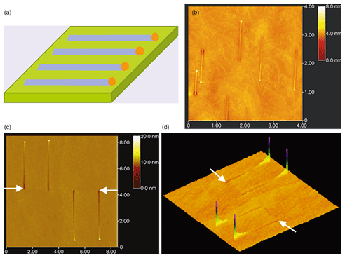
6. Novel structure––planar nanowiresFor the integration of nanowire-based devices, we need aligned nanowire arrays with vertical structures or ex-situ assembly methods that align randomly distributed nanowires into a planar array for subsequent device fabrication. However, contamination introduced during the ex-situ process may degrade device performance. The ideal way to achieve simple nanowire integration is to grow a planar nanowire array by an in-situ process. A schematic diagram of planar nanowires grown laterally on a substrate by the particle-catalyzed VLS method is shown in Fig. 9(a).
We have successfully developed an approach for growing planar GaAs nanowires using the Au particle-catalyzed VLS method. An atomic force microscope (AFM) image of GaAs nanowires grown laterally on a substrate by this technique is shown in Fig. 9(b). We can clearly see the particles at the nanowire tips. Further experiments indicated that the lateral nanowires could be well controlled in terms of size, site, and density. Here, we show an example of planar nanowire site-control by defining the Au particle positions by electron beam lithography. AFM images of planar nanowires grown from linearly aligned Au particles, whose initial positions are indicated by white arrows, are shown in Figs. 9(c) and (d). Note that the Au particles moved to the nanowire tips in two directions [10]. The high controllability will allow device applications including conduction channels and optical elements. We expect the planar nanowire structure to provide new opportunities for the development of novel 3D nanostructures and highly efficient photonic devices with size- and site-controlled quantum dots. 7. ConclusionWe have shown that semiconductor nanowires offer many opportunities for fundamental research and for applications to nanoscale electronic and optoelectronic devices. The 1D nanoscale semiconductor structure may lead to a breakthrough in certain technological problems such as the integration of III-V compound semiconductor devices with Si-based technology. We have established a state-of-the-art nanostructure (device) fabrication technique by using a bottom-up approach and have synthesized novel nanostructures for fundamental quantum optical and transport phenomena research. Central to our progress in the field and our future efforts at achieving applications is the rational control of the key growth parameters of the nanowires, including their chemical composition, structure, size, morphology, and doping, since it is these parameters that determine whether or not we achieve the desired device functions. Looking to the future, we believe that continued advances in our ability to control the structural/compositional complexity of nanowires will lead to unique nanoelectronic and optoelectronic circuits and systems that will help us create the technologies of the future. References
|
||||||||||||||||||||||||||||||