|
|||||||||||||||||||||
|
|
|||||||||||||||||||||
       |
Feature Articles: System LSI Design for Broadband Optical Access Network Systems Vol. 9, No. 3, pp. 11–16, Mar. 2011. https://doi.org/10.53829/ntr201103fa2 Cooperative Hardware/software Design TechnologyAbstractIn this article, we introduce a hardware/software co-design simulation method for testing the cooperative design of hardware and software for system-on-a-chip (SoC) devices. For SoCs, which incorporate dedicated processing circuits and a processor, combined testing of the software running on the processor and the operations of the dedicated circuits must be done from the initial design stages in order to reduce the amount of redesign and the turnaround time, i.e., the number of person-hours of work required. Our cooperative simulation method uses virtual hardware. We discuss its effectiveness by referring to real examples. 
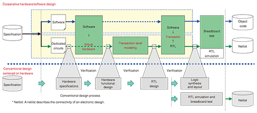
1. IntroductionIn the design of system-on-a-chip (SoC) devices, it is extremely important to design so that the hardware, which handles specialized processing, and the software running on the microprocessor, operate cooperatively. In other words, the design process must also be cooperative. How can this be tested? The microprocessor operates according to what is written in its program (software). On the other hand, the dedicated processing circuits process data continuously according to how the hardware has been designed and a clock signal. Thus, the operation of the two must be checked to ensure that they do not cause a conflict, mismatch, deadlock, or other type of performance drop. This is cooperative design evaluation. The evaluation results can affect the system architecture greatly, so such an evaluation must be done from the initial stages and from the top level of design. However, at the top-level design stage, there is no actual hardware. It would be nice to build an overall prototype including both the microprocessor and dedicated circuits, put them together and test them, but development usually cannot wait for this. Systems being implemented as SoCs have recently become extremely complex, so that even building or rebuilding a single prototype can take several weeks or months. For this reason, it has become necessary to simulate the hardware together with the system software before prototyping it; in other words, one must perform a hardware/software co-design simulation. 2. Virtual hardwareTo implement co-design simulation, we need a simulator for virtual hardware. Physical hardware operates with a clock signal for input and output to the dedicated circuits so the processor can read from and write to it, but virtual hardware does not have a physical clock. Instead, attention must be paid to the sequencing and dependencies of reading and writing and to the input and output between the processor and dedicated circuits, and the simulator must be built to maintain these relationships. Before the design of the dedicated circuits is complete, one does not know how many clock cycles will be required for these circuits to complete their operation. However, the correct sequencing and dependencies for reading and writing are correctly coded in the virtual hardware, so the virtual hardware can respond to the software behavior without conflict. This makes co-design simulation possible from the top-level design stages. 3. Issues being addressedWe have applied this type of co-design simulation using virtual hardware to the evaluation of SoC designs for optical access systems. As a result, we have confirmed the usefulness of the method. The new process is shown in Fig. 1 together with the conventional design process. The lower half of the figure shows the conventional design process centered on hardware. Here, the hardware was the only specification to achieve. However, in hardware/software co-design, which allows cooperative testing with the software, part of the specification is achieved with software. The hardware/software co-design process can handle a wider specification range than the conventional design process. Moreover, whereas the conventional design process creates a hardware netlist, the cooperative design process creates two netlists—one for the dedicated circuits and another that connects the processor and dedicated circuits—and software object code that controls the processor’s behavior. Therefore, Specification and Netlist are grayed out in the lower half of Fig. 1 because they cover different ranges to those in the upper half.
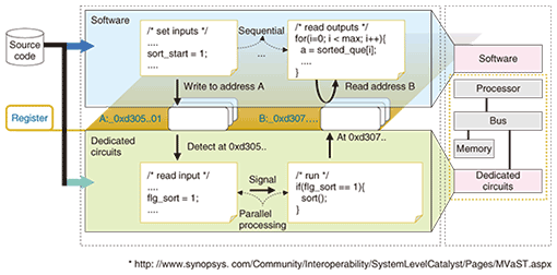
The dedicated circuits are designed according to the conventional hardware design process: they become more detailed in three stages from specifications to functional design and register transfer level (RTL) design. Software cooperative testing (verification) can be done at each of these three stages by using co-design simulation with virtual hardware. We started by building the virtual hardware (leftmost green box in Fig. 1.) for the initial stage (specification design). This allowed early verification of the SoC software. Then, at the intermediate stage (functional design), we addressed the hardware transaction-level design (second green box). This can be simulated several times faster than when designing in detail to the RTL level. Finally, at the RTL design stage, we built a mechanism called a transactor (third green box) into the system for sections connecting the dedicated circuits with the processor. This enables precise final verification of the interfaces between hardware and software in the SoC. 4. Construction of virtual hardwareWe verify the software at the specification design stage with the goal of determining aspects such as whether adequate performance is achieved and whether performance will drop owing to interference with the dedicated circuits. The software is not executed independently, but loaded on the original SoC architecture, which includes both the processor and dedicated circuits. Thus, we have built virtual hardware that simulates the entire SoC, as shown in Fig. 2.
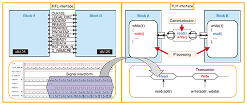
The key to building virtual hardware is the separate parts for software and dedicated circuits, which are where the processing that defines the functional characteristics of the SoC takes place. For our optical-access SoC, these characteristics were the ability to interface with sophisticated, high-speed communication lines. The specifications for these components are complex, so they were expressed not only in documents, but also as source code in the C programming language. To ensure that the implementation was faithful to the specifications, we built the dedicated circuit part of the virtual hardware by directly using this C source code as far as possible. The source code includes both the software that will be loaded by the processor in the SoC and the software representing the dedicated circuits. Communication between them uses registers, which create the correspondence between variables in the software and variables for the dedicated circuits, so the address-mappings for these registers must be managed. The mechanism of communication between software and a dedicated circuit conducted via a register is shown in Fig. 2. When the software side writes to address A, the dedicated circuit side detects it as being written at address 0xd305… (in hexadecimal). Because the dedicated circuit is always processing, the influence of the write will sooner or later be written at address 0xd307…, which is equivalent to Address B on the software side. The software side reads values from Address B according to the execution order and conditional judgment. The dedicated circuit reads the value that was written earlier to Address B, and, as a result of the dedicated circuit procedure, its behavior when it reads Address B reflects the software side. The number of these registers is generally very large. Most of the specification is related to these registers, so any updates to the specifications can involve a significant amount of rewriting in the virtual hardware. This results in additional design work, so we used data structures, which allow us to manage all of the registers at once and make it easy to apply updates to the specification. This approach can be generalized, decreasing the amount of time required from confirmation of the specifications to system-level operation. For the current project, we were able to detect routines that were performing inadequately several months before beginning verification of the physical hardware. 5. Transaction-level designIn the same way that software performance can be checked using virtual hardware, the dedicated circuits can be simulated at the functional design stage. This simulation is faster than RTL-stage simulation, but it must be done using transaction level modeling (TLM) to describe the transaction-level design. In the past, for functional design simulations, each of the lines between modules would be simulated individually and in complete detail, down to individual clock cycles. This resulted in a number of problems. First, a lot of work was required to complete the detailed design before simulation could begin; moreover, component redesign because of interference with other blocks could have a major effect on the design schedule [1]. Second, a detailed simulation could not be executed quickly and consumed much time. Third, the test coverage was difficult to manage [2]. To resolve these difficulties, we used SystemC [3] TLM to structure the design file for the dedicated circuit section. At the functional design stage, testing must verify points where data is exchanged between blocks. The TLM interface between blocks A and B is compared with the RTL interface in Fig. 3. When a block passes the results of its processing to another block, the procedure can be very long, as in the RTL case on the left. However, this procedure can become very simple, as shown on the right side, if the exchange is rewritten as a transaction. A transaction is the core action, such as the start or confirmation of a transmission or reception. The events handled in a simulation using TLM are arranged beforehand, so simulation can be done at high speed. When TLM is used, descriptors for the lines connecting blocks are much shorter, and this effectively reduces the amount of preparation work for simulation. Overall, the amount of descriptor code was about one-tenth of that for RTL, and the simulation executed about 100 times as fast as the RTL simulation.
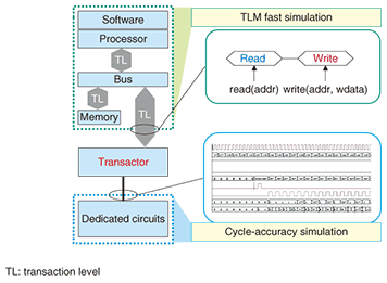
6. Built-in transactorsCompleting an RTL design of the dedicated-circuit section enables precise simulations to be done in block units, but problems arise when cooperative simulation is performed. The processor in the virtual hardware does not have actual signal lines, so the RTL for the dedicated circuit section cannot be connected to the virtual hardware as it is. Thus, we built transactors into the virtual hardware, as shown in Fig. 4. Transactors are composed of libraries provided by the existing simulation infrastructure [4]. We used library functions to code the transactor to monitor accesses to the bus by the RTL of the dedicated circuits. When an access is detected, a function updates the register value at the appropriate address. Figure 4 shows a transactor connecting two simulators: the lower one simulates the dedicated circuits with cycle accuracy and the upper one simulates the software-equipped processor with fast TLM. The grey areas labeled TL (transaction level) mean that a TL connection is used when these areas are simulated. In the processor and bus in this area, when each part performs communications with the other part, the performance is set using a TL write. The TL connection enables communications to be performed with transaction between connected parts (models) and leads to high-speed simulation. On the other hand, the area of dedicated circuits is written to enable simulation with more detailed cycle accuracy. There is no way to connect directly between an area that uses TL connection when simulated and another area simulated with cycle accuracy because the input/output signal formats are completely different. That is why a transactor plays the role of a mutual conversion function for the two communication methods.
With the earlier approach, we built a prototype board, reproduced the RTL on a field-programmable gate array (FPGA), and loaded the software onto the processor to evaluate the whole system. The data for writing the FPGA was created using computer-aided design, and this also required several weeks of preparatory work. In comparison, using the new method, the design for this project required only five person-days of preparation before evaluation was started. The method cannot replace all of the testing done with a prototype board, such as realtime signal processing, but final testing can be started several weeks earlier; the saved time is the time that would have been required to prepare the data for rewriting the board. 7. Cooperative design technology in the futureIn this article, we introduced an example of applying cooperative design methods to the design of an SoC for optical access. Through this example, we showed that system-level cooperative simulation, at a level of precision appropriate and relevant for design stages as they progress, is possible for the dedicated circuit components, from top-level design to the final processes. In the future, it will become more important to do multistage cooperative simulation, from the beginning and in accordance with the design stages, when designing SoCs. The future possibilities enabled by this sort of design methodology are not limited to SoCs. Large-scale systems of even more complexity will fall into the scope of this research and we are taking on this new challenge. References
|
||||||||||||||||||||