|
|||||||||||||||||||||||
|
|
|||||||||||||||||||||||
       |
Feature Articles: System LSI Design for Broadband Optical Access Network Systems Vol. 9, No. 3, pp. 17–22, Mar. 2011. https://doi.org/10.53829/ntr201103fa3 MAC LSI Design Technology for Optical Access CommunicationsAbstractIn this article, we explain the development process and architecture of a media access control (MAC) large-scale integrated circuit (LSI). The MAC LSI is a very important component that provides most of the functions of an optical line terminal and optical network unit, which are the main devices in an optical access system. The required functions include the passive optical network interface, buffers, bridges, and maintenance & authentication. 
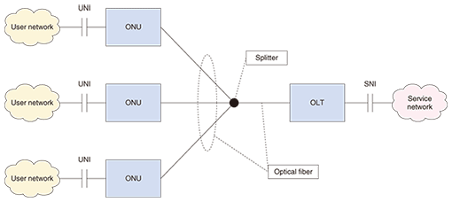
1. IntroductionThe development of a large-scale integrated circuit (LSI) begins with the definition of requirements. For this, the specifications of the systems in which the LSI will be used must first be decided appropriately. A media access control (MAC) LSI is a very important component in an optical access system because these LSIs provide most of the functions of the optical line terminals (OLTs) and optical network units (ONUs), which are the main devices. The MAC LSI is classified as a system on a chip (SoC) because it contains a central processing unit (CPU), memory, and large-scale dedicated logic circuits. When MAC LSI development begins, many details of the service and system specifications are still undecided, so while the specifications are being decided, close communication must be kept with internal departments studying the next-generation systems. For each system function, one must decide whether it will be implemented in the LSI or by using external components. As many functions as possible should be placed in the LSI to reduce the number of external parts and hence the equipment cost. However, as the number of functions in the LSI increases, the cost of the LSI itself also increases, so a good balance must be found. Requirements other than functionality must also be decided appropriately, including power consumption targets or performance parameters such as frame processing speed and processing time. 2. LSI designAfter the LSI requirements have been decided, one must decide which of the functions are to be implemented in hardware and which in software. Generally, functions that require high performance are implemented in hardware, and ones that require a flexible configuration are done in software. For a MAC LSI, functionality must be allocated to satisfy the requirement that all input frames can be processed, without the speed dropping below the wire speed. Once the hardware/software assignments have been decided, their designs can proceed. We try to keep the hardware design as small as possible while meeting the performance requirements, but we must also consider the following points: (1) Each function should be able to be modified flexibly through configuration. This is so that, for example, if standards have not been finalized at the development stage, they can be accommodated even if they do change without the hardware needing to be rebuilt. (2) At the beginning of development, in particular, in addition to the functions required for services, testing and debugging functions needed during development should also be provided. Examples of functions of this sort are a loopback for the main signal, various counters, and internal signal monitoring functions. The software can be categorized into components that access the hardware and those that do not, and the software design can proceed more smoothly if the hardware-accessing components are designed as application programming interfaces. 3. Coding and verificationThe next part of the design is coding. For the hardware, we use a register transfer level (RTL) description with a hardware description language such as Verilog-HDL. For the software, we mainly use the C language. Coding is followed by verification testing. Once the hardware has been built, making further changes is extremely expensive and time consuming, so testing must be done before production to eliminate as many problems as possible. For the hardware, in addition to using logical simulation to check operations, we check some of the functions by actually running them using field programmable gate arrays (FPGAs) to emulate the hardware. Verification using FPGAs is discussed in detail in the fourth Feature Article in this issue, “Design Verification Using Field-programmable Gate Arrays for Optical Access Communications SoC” [1]. The operation of the software must ultimately be checked on the actual hardware, but as hardware and software development proceeds in parallel, the software must be tested as far as possible before the hardware is complete. For this purpose, a software model simulating the hardware is created. This is discussed in detail in the second Feature Article in this issue, “Cooperative Hardware/software Design Technology” [2]. When testing is complete, a logic-synthesis tool is used to create a netlist* from the RTL description. Once the RTL description has passed all testing, it is called the clean file, and a netlist created from this clean RTL description is passed to an LSI manufacturer for outsourced production. 4. MAC LSI architectureHaving given a step-by-step explanation of the LSI development process above, we now describe the architecture of the optical access communications MAC LSI. There are several optical access methods, but as an example, we describe EPON (Ethernet passive optical network) here. There are two types of EPON [4], [5]: GE-PON (Gigabit Ethernet passive optical network) with a frame rate of 1 Gbit/s and 10G-EPON at 10 Gbit/s, but most of the following description applies to both equally. An overview of the EPON system is shown in Fig. 1. It is composed of an OLT, ONUs, optical fibers, and splitters. The OLT, which is usually in the provider’s central office, is connected to the service network through the service node interface (SNI), and an ONU, which is usually on the user’s premises, is connected to the user network through the user network interface (UNI).
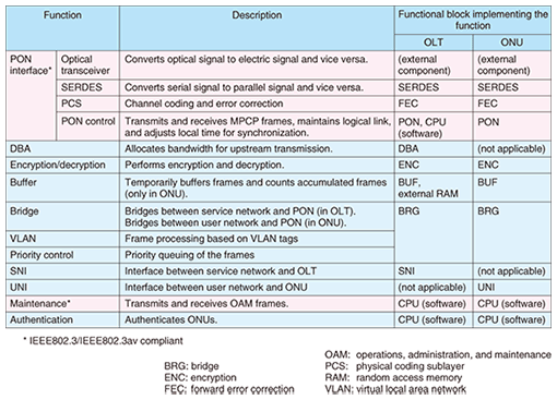
The functions required by the OLT and ONU, with explanations, are given in Table 1. Each of these functions must be implemented either in the LSI or by using external components. For LSI implementation, each function is designed in a cluster called a functional block. The correspondence between functional blocks and these functions is shown in Table 1. The functional blocks are divided into two types: (1) functional blocks that receive, process, and transmit frames and (2) other functional blocks.
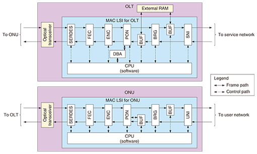
In Table 1, the dynamic bandwidth allocation (DBA) and CPU sections are of type (2) and the rest are of type (1). The MAC LSI architecture can be formed by arranging the type (1) functional blocks in the order of frame flow, and connecting type (2) blocks to the blocks that they control. Examples of OLT and ONU implementations using an LSI with this architecture are shown in Fig. 2. As shown clearly in Table 1 and Fig. 2, most of the functions of both OLT and ONU are implemented in the MAC LSI.
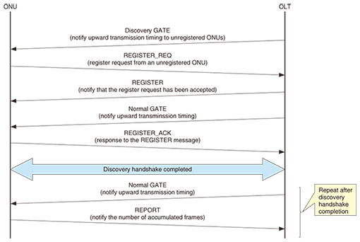
The MAC LSIs for the OLT and ONU in Fig. 2 have similar structures, but although they may share the same name for a functional block, there are differences in the functional blocks of the OLT and ONU, as described below. (1) Within the EPON system, multiple ONUs connect to a single OLT, so all blocks except the SERDES (serializer/deserializer), SNI, and CPU in the OLT MAC LSI must be able to handle multiple ONUs. (2) To implement the PON control function, the PON components of the MAC LSI for OLT and ONU must each transmit and receive control frames according to the well-defined sequence for each. The PON control function is described later. (3) Uplink bandwidth allocation is required only in the OLT, so only the OLT has the DBA block. Conversely, the ONU must notify the OLT of accumulated frames, so the accumulated frame calculation function is present only in the buffer (BUF) section of the ONU. (4) In the PON section for EPON, the downlink is a continuous signal, but the uplink is a burst-mode signal, so the ONU transmitter and the OLT receiver must support burst-mode communication. Burst-mode communication is described in detail in the fifth Feature Article “10-Gbit/s Burst-mode Receiver Integrated Circuits for Broadband Optical Access Networks” [5]. 5. PON control functionThe PON control function is an important function that administers the OLT-ONU links. When a new ONU connects to the PON, the PON control functions of the OLT and ONU establish a link by exchanging multipoint control protocol (MPCP) control frames in the sequence shown in Fig. 3. The process by which a newly connected ONU establishes a link is called discovery. Once discovery has been completed, MPCP control frames are exchanged periodically for link maintenance.
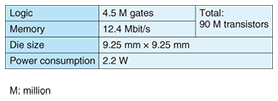
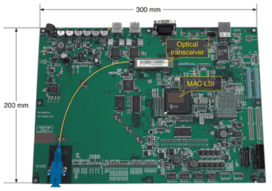
EPON uses time-division multiple access on the uplink, so the OLT and ONU must be synchronized, and this is also done by the PON control function. With EPON, the OLT internal clock acts as master, and ONUs are notified of the time by the transmit timestamp set in MPCP control frames. ONUs receiving this notification adjust their clocks to match. This can produce some jitter in the ONU clocks, so the ONU’s PON control function must be designed not to malfunction owing to clock jitter. 6. Example of MAC LSI prototypeWe have built a prototype LSI for a GE-PON ONU as described here. Details of the prototype are given in Table 2, and a photograph of the LSI mounted on an evaluation board is shown in Fig. 4.
7. Conclusions and future developmentsWe described the development process and architecture for a MAC LSI for optical access communications and introduced a prototype of the LSI. 1-Gbit/s services using the GE-PON optical access system have been commercialized. However, the 10-Gbit/s rate for 10G-EPON has already been standardized, and even faster systems are expected in the future. LSI operation speeds are expected to increase slowly in comparison with these data transmission rates, so new architectures may be needed to handle the rising network speeds. Equipment cost reduction and power consumption control will also continue to increase in importance, so technical development be needed for their achievement. Finally, as functionality becomes more complex, the scale of LSIs needed for networking will continue to increase, so design technology and tools to handle larger-scale LSIs will also need to be developed. References
|
||||||||||||||||||||||